Download the PDF file
Background
The following contains a brief
description of isolation technologies used for radiation hardened integrated
circuits. The technologies mentioned are junction isolation, Dielectric
Isolation (DI), Silicon on Sapphire (SOS), and Silicon on Insulator (SOI). The
report is intended to be informational. The results of Internet searches and
interviews with Code 605 personnel involved with the Strategic Systems Program
were the primary sources of information. The Strategic Systems Program relies
on these non conventional isolation techniques for radiation hardened integrated
circuits.
Executive Summary
For over 40 years
junction isolation has been the primary technology used to isolate the
individual components on integrated circuits. Early alternate technologies such
as DI, SOI, and SOS were driven by their ability to tolerate radiation. There
are relatively few applications for radiation hardened parts therefore the
demand for DI, SOI, and SOS has been quite small. DI, SOI, and SOS wafers
accounted for a very small portion of the worldwide Silicon wafer production
prior to 2000. In the late 90’s the demand for high speed VLSI Integrated
Circuits was pushing junction isolation to its technological limits. The
performance advantages of thin film Silicon on Insulator (SOI) integrated
circuits brought about improvements in SOI. This resulted in an increased
demand for SOI wafers. Semiconductor Equipment and Materials International
(SEMI) estimates that SOI wafer sales doubled to $405 million in 2005.1 Yet SEMI estimates
that was less than 5% of Silicon wafers sales worldwide. SEMI predicts that
sales will reach $911 million by 2009. The worldwide demand for high
performance integrated circuits has produced a reliable source for a
commercially available radiation tolerant semiconductor manufacturing
process.
Introduction
Monolithic Integrated Circuits
(ICs) have traditionally utilized junction isolation as a means of electrically
isolating individual active and passive devices on the IC. Individual devices
are diffused into a substrate. A reversed biased P-N junction between the
substrate and individual devices provides the isolation between devices. The
process is well established, reliable, and economical.
DI, SOI, and SOS make use of an
engineered wafer. The IC manufacturer buys a wafer that has been manufactured
with an insulating layer beneath the active Silicon. These wafers can be
engineered to replace the standard bulk Silicon wafers in a conventional
junction isolation IC manufacturing process. An IC isolated by a dielectric
such as Silicon Dioxide (SiO2) or Sapphire
(Al2O3) has advantages over its junction isolation
counterpart. Three of the main advantages are immunity to radiation, lower
leakage currents, and higher operating frequency all due to the elimination of
junction isolation.
Photocurrents generated by
ionizing radiation in junction isolation can impact an integrated circuit in
many ways. Photocurrents are reduced by dielectric isolation. The main benefit
of dielectric isolation is the elimination of LATCHUP (LATCHUP is the
inadvertent creation of a parasitic Thyristor structure in an Integrated
Circuit). A switch to DI, SOI, or SOS can dramatically improve an IC’s
immunity to Prompt Dose radiation or Single Event Effect radiation. There are
many factors to consider when designing a radiation tolerant integrated
circuit. Switching a process to DI, SOI, or SOS is not a guarantee that the IC
will be radiation tolerant. The dielectric that improves Prompt Dose and Single
Event response may trap charge and degrade the Total Dose response unless
additional processing steps are taken. Several processing and design techniques
must be utilized to guarantee a radiation tolerant IC. Some of these can also
be used to improve the radiation tolerance of junction isolation technologies.
Dielectric isolation doesn’t have
the leakage current to substrate that junction isolation does. The leakage
current of a reverse biased P-N junction increases with temperature. This can
limit the maximum operating temperature of IC’s utilizing junction
isolation.
Reversed biased P-N junctions
possess an inherent capacitance. This parasitic capacitance limits the
operating frequency of an IC. The parasitic capacitance of a dielectrically
isolated part is lower than that of one utilizing junction isolation. This
gives dielectric isolation a performance advantage versus its junction isolation
counterpart. It enables a dielectrically isolated part to operate at higher
frequencies and lower power. This performance advantage is currently the main
driver for commercial SOI technology.
Technologies
DI
Technically DI, SOS, and SOI are all dielectric isolation. In this
discussion DI refers to a specific isolation technique that is different from
SOI and SOS. DI processes, often referred to as poly DI, have been used for
over 30 years in radiation environments.
DI processing typically begins
with an N+ type wafer. An N type Epitaxial layer is grown on the wafer. Masked
N and P diffusions form islands for the individual devices. The individual
devices are isolated by etching moats around the islands. The moats extend down
to the N+ starting wafer. A thick oxide is grown that forms the isolation on
the sides and bottoms of the devices. A thick layer of Poly-Silicon is
deposited to fill in voids and add strength. The Poly-Silicon will be the
substrate for the finished device.
The N+ starting wafer is removed
by abrasive polishing. Modern DI processes use a final electrochemical etch
that automatically stops at the lower doped Epitaxial layer; this allows the
thickness of the final islands to be determined by the Epitaxial process. The
remaining dielectrically isolated islands can be processed into integrated
circuits.
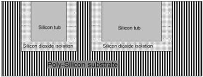
Figure (1) is a simple diagram showing a cross section of a DI wafer. DI is a
mature process. It is well suited for high voltage applications (MOS Vgs
to150V, BJT BVceo to 35V). It is a relatively low frequency
technology due to lack of additional development. The process does not produce
a uniform thin film of Silicon needed for high performance integrated circuits.
Wafer warping has limited the size of the wafers to 4 inches. It is not certain
how long IC manufacturers will continue to produce DI.

Figure (1) Diagram of Dielectric
Isolation Cross Section
SOS
SOS refers to
Silicon on Sapphire. The active Silicon device is formed on an electrically
insulating crystalline Al2O3 (Sapphire) substrate. An
Epitaxial layer of Silicon is grown on a crystalline Sapphire wafer. Subsequent
Ion implantation and heat treatment produce a thin silicon film suitable for
high performance IC fabrication.
During IC fabrication islands of
Silicon are formed by patterned oxidation of the Silicon film. The islands of
Silicon are isolated laterally by Silicon Dioxide that extends to the Sapphire
substrate. Sapphire is one of the few insulating substrates that single crystal
Silicon can be grown on. Figure (2) is a diagram showing a cross section of an SOS wafer.
SOS technology has
been developing since the 1960s. In the beginning it was plagued by the lattice
unconformity between the crystalline Silicon and crystalline Sapphire. The
unconformity created lattice defects in the Silicon. Diffusion of Aluminum from
the Sapphire into the Silicon was also a problem. Improvements in technology
have made SOS more reliable and accelerated the development since the 1990’s.
SOS can have excellent Prompt Dose and Single Event Effect radiation immunity.
High quality passive components such as inductors can be constructed on it. An
additional advantage is that the translucent sapphire wafer allows for
implementation of high performance optical interconnect communication. This can
accomplished using Vertical Cavity Surface Emitting Lasers (VCSEL) and coupling
through the substrate. Flatness of Sapphire wafers is somewhat inferior to
Silicon wafers.2 This has
discouraged large area high integration circuits from being fabricated on
SOS.

Figure (2) Diagram of Silicon on
Sapphire Cross Section
SOI
Technically
DI could be considered Silicon on Insulator (SOI). In this discussion SOI
refers to integrated circuits that consist of a thin film of single crystal
Silicon separated from the bulk substrate by a layer of insulating Silicon
dioxide. Several vendors, including IBM, National Semiconductor, Honeywell,
Advanced Micro Devices and Intel, are currently supporting SOI processes. The
performance of an SOI device relies on the ability to fabricate a thin film of
defect free single crystal Silicon. Currently there are two approaches that
have been widely used for manufacturing SOI starting wafers. One method is
known as Separation by Implanted Oxygen (SIMOX) and the other is wafer
bonding. Oxygen ions are implanted into Silicon to form the Silicon dioxide
layer in the SIMOX process. The energy and dose rate of the implant control the
depth and thickness of the oxide layer. The oxide layer forms after a high
temperature annealing. The annealing does not remove all of the lattice damage
from the implanted Oxygen. Silicon pipes from the active silicon layer through
the oxide to the substrate are also a problem. Current processes have reduced
defect levels to acceptable levels. Lateral devices fabricated on SIMOX wafers
are less affected by Silicon defects than vertical devices. SIMOX is well
suited for high performance low voltage CMOS integrated
circuits.
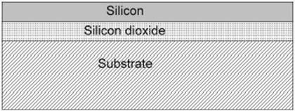
Figure (3) is a diagram showing a cross section of a SIMOX wafer. Patterned
local oxidation of the Silicon film during IC fabrication defines the lateral
isolation of the individual IC components.

Figure (3) Diagram of SIMOX Cross
Section
Wafer bonding avoids the damage
caused by implanted Oxygen. The oxidized surfaces of two Silicon wafers are
bonded. Part of one of the wafers is selectively removed to leave a thin
uniform layer of crystalline Silicon on top of an insulating layer of Silicon
dioxide. Patterned local oxidation of the single crystal Silicon film forms the
lateral isolation. Wafer bonding is well suited for high performance CMOS,
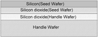
BiCMOS and higher power devices. Figure (4) is a diagram showing a cross section of wafer bonded
SOI.
A patented
process called Smart Cutâ is a very promising wafer bonding technique.3 Smart Cutâ starts
with an oxidized seed wafer. Hydrogen is implanted into the Silicon wafer
through the oxide. The depth of the implant is controlled by the implant
energy. The seed wafer is aligned and bonded to a handle wafer. The bonded
wafers are heated in an oven. The heating causes the wafers to split along the
Hydrogen implanted plane. The result is a thin film of crystalline Silicon from
the seed wafer resting on an insulating Silicon dioxide layer. The handle wafer
provides strength and support for the finished product. The remaining seed
wafer can be used again.

Figure (4) Diagram of Bonded Wafer Cross
Section
Smart Cutâ was
developed at CEA-LETI; an applied research laboratory operated by the French
Atomic Energy Commission. Soitec obtained an exclusive license for the initial
Smart Cutâ patents. Soitec now supplies nearly 80 percent of the
worlds SOI wafers.1 Soitec is planning
to construct a new factory capable of producing 1 million 12 inch SOI wafers
yearly. The plans call for the factory to be producing wafers by 2008.
Concluding
Remarks
All
of the aforementioned technologies have advantages and disadvantages. Table (1) compares some of their features. DI and
SOS still have their niche applications. Bulk Silicon wafers using junction
isolation will most likely dominate the semiconductor industry for many more
years. Bonded wafer SOI has entered the mainstream and will continue to
increase its market share. This should create a reliable source for bonded SOI
wafers and make SOI an attractive technology for radiation tolerant devices.
Any radiation tolerant design should consider if the technology used will be
available for the life of the system. The Strategic System Program is relying
on bonded wafer SOI technology for most of their future applications. For
questions, NSWC Crane POC is 812-854-2105.
|
|
|
SOI
|
SOS
|
DI
|
Bulk
|
|
Price
|
|
High
|
High
|
High
|
Low
|
|
|
|
|
|
|
|
|
Technologies
|
Bipolar
|
Good
|
Poor
|
Good
|
Good
|
|
|
C-MOS
|
Good
|
Good
|
Good
|
Good
|
|
|
High
Voltage
|
Fair
|
Good
|
Good
|
Good
|
|
|
Bi-CMOS
|
Good
|
Poor
|
Fair
|
Good
|
|
|
Passive
Devices
|
Fair
|
Good
|
Fair
|
Fair
|
|
|
|
|
|
|
|
|
Radiation
|
Total
Dose
|
Good
|
Fair
|
Good
|
Good
|
|
Environment
|
Prompt Dose
|
Good
|
Good
|
Good
|
Poor
|
|
|
Single
Event
|
Good
|
Good
|
Good
|
Fair
|
|
|
|
|
|
|
|
|
Performance
|
High
Speed
|
Good
|
Good
|
Fair
|
Good
|
|
|
High
Voltage
|
Fair
|
Good
|
Good
|
Good
|
|
|
Low
Power
|
Good
|
Good
|
Fair
|
Fair
|
Table (1)
Feature
Comparison
Bibliography
1 Russ Arensman, Engineering
Design News/Electronic Business, EDN.com,, 7/1/2006
2 Toshiyuki Nakamura, et al.,
Oki Technical Review, October 2004/Issue 200 Vol.71 No.4, pg. 69
3 G.K. Celler and Sorin
Cristoloveanu, Journal of Applied Physics, May 2003, Volume 93, No. 9, pg.
4962