Download the PDF file
Introduction
The purpose of this document is to
familiarize the user with the basic concepts of a de-rating analysis, starting
with circuit analysis and proceeding through documentation. Electrical stress
de-rating analysis is the process of determining a part's ability to withstand
induced stresses under given environmental conditions. Induced stresses are
taken from the datasheet and circuit analysis, and are identified in terms of
voltage, current, power, etc. Environmental conditions refer primarily to
temperature and are taken from the system's operating requirements.
One of the objectives of a stress
analysis is to provide early warning of design deficiencies at the time in the
program phase where changes are least expensive (i.e., while the design is still
on paper). A stress analysis incorporated early into a program can significantly
reduce test time and cost by providing a basis for a reliable design.
Transient conditions must also be
taken into account. The analysis will not necessarily consider worst case
conditions with regard to applied voltages or currents, part parameter values,
or driving signals. However, when an undesirable stress condition is noted,
worst case conditions should be examined and the probability of worst case
occurrence investigated.
Preliminary Analysis
Prior to performing a stress
de-rating analysis, a thermal analysis and circuit analysis must first be
completed. Circuit analysis is considered outside the scope of this document. In
brief, circuit analysis is the process used to calculate the electrical
parameters of each part in the circuit, such as voltage, current, power,
etc.
Determining Part Stress
Ratings
After thermal and electrical
parameters are known, it is possible to calculate part stress ratings. The part
stress rating is defined as the ratio of applied to rated electrical parameters.
These electrical parameters may consist of voltage, current, power, inverse
voltage, etc., or any combination, depending on the part. For example, a power
stress ratio is used for a resistor, while a voltage stress ratio is used for a
capacitor.
A part's stress rating can vary
from lot to lot, vendor to vendor, application, and nearly always increases with
increasing temperature. This document will concentrate on the latter; that is,
how to calculate stress ratings with increasing temperatures. It will do this by
presenting examples. For the purpose of these examples, it is assumed a thermal
profile analysis has already been done in accordance with the Thermal Analysis
document.
Examples
Example #1: Application of a Solid
Tantalum Capacitor Voltage Rating
Given:
a. The device is a 6.8
mf
electrolytic tantalum capacitor. Device ratings according to the
datasheet are shown in Figure 1.
Maximum rated operating voltage is 25 VDC up to 85oC. Absolute
maximum operating temperature (TMAX) is 125oC. The device
is rated for operation up to 16 VDC of maximum operating at 125oC.
b. Maximum equipment external ambient
temperature profile is 70oC. The internal temperature rise in the
equipment was determined to be 30oC using the principles of the
Thermal Analysis document.
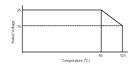
Figure 1: Maximum Voltage Rating for
Electrolytic Tantalum Capacitor, Example #1
c. Maximum impressed voltage is 10 VDC,
determined from the electrical circuit analysis.
Determine:
a. The maximum voltage rating of the
capacitor at the operating temperture.
b. The required capacitor voltage rating
using the derating requirements in this manual.
Solution:
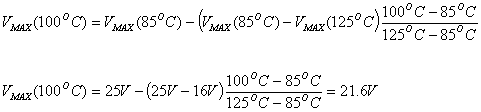
First, determine the part ambient
operating temperature (Top). This is the sum of the external
ambient equipment temperature (70oC) and the internal temperature
rise (30oC) or,
Top = 70oC +
30oC = 100oC
At an operating temperature of
100oC, the maximum part rating is determined by one of formulas,
depending on the operating temperature (Top):
 |
Eq-1 |
The operating temperature (Top) given in the
example (100oC) is between Ts (85oC) and
TMAX (125oC), so the center equation is
used. Substituting:
O some users prefer to use the slope version of the formula
instead, as follows, which yields identical results:
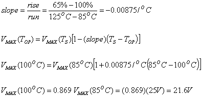 |
Eq-2 |
For the solution to part (b) of the question, first
determine the derating guidelines for tantalum capacitors. The derating
guidelines for electrolytic tantalum capacitors 60% to Ts, and
then linearly derated to TMAX - 10oC. This
is reproduced in Figure 2.
Also shown is the operating temperature of the capacitor along with its maximum
allowed stress ratio.
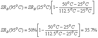
The maximum derated Stress Ratio
(SRD) at the operating temperature is calculated by the
formula:
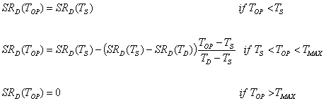 |
Eq-3 |
(Note this is identical to Eq-1 on the previous page except
stress ratio is substituted for voltage.)
Substituting:
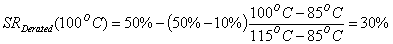
The current 25V capacitor therefore does
not meet the derating guidelines. The derated maximum rating is greater than the
actual voltage the capacitor is expected to see, or:
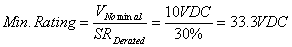
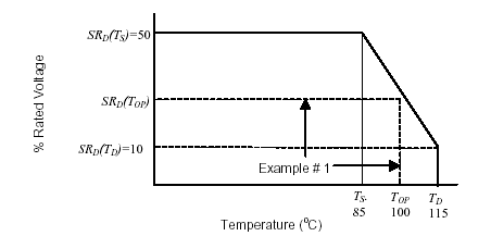
Figure 2: Derating Requirements For
Electrolytic Tantalum Capacitor,
Example #1
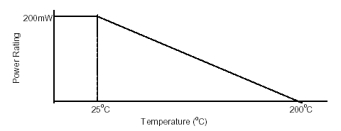
Figure 3: Maximum Power and Temperature
Ratings Transistor,
Example #2
To meet the derating guidelines, a
capacitor with a voltage rating of at least 33.3 VDC is required, calculated as
follows:

The proper capacitor is 6.8 mf,
35 VDC rated.
Example #2, Application of a
Transistor
Given:
A user requires a transistor to be used in
an application where it will be required dissipate 70 mW of power. Ambient
temperature (TA) in the immediate vicinity of the transistor is
50oC.
The selected transistor has maximum power
dissipation ratings shown in Figure 3.
The transistor can dissipate up to 200mW at 25oC. Above
25oC, the datasheet requires the maximum power dissipation rating to
be linearly "derated" to a maximum junction temperature (TJ) of
200oC. The transistor has a thermal resistance (QJA)
from junction to ambient of 0.875oC/mW.
Determine:
Determine if the selected resistor can be
properly derated for the given application using the derating guidelines of this
document.
Solution:
The derating guidelines for a silicon
transistor are reproduced in Figure 4.
Ts and TMAX are taken from the datasheet and the given
information. Ts is the maximum operating temperature at which full
rated power can be applied, or in this case 25oC. TMAX is
the maximum junction temperature (TJ) or absolute
maximum temperature at which the part can operate. In this case, it is
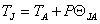
200oC. Maximum derated temperature (TD) is then
calculated by the formula:
Substituting,
 |
Eq-4 |
The derating curve is now completely
defined and shown in Figure 4.
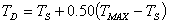
Next, determine the derated stress ratio
(SRD) allowed by the derating guidelines. Equation #3
is again used, except it is simplified because the derated stress ratio is zero
at TMAX, or
 |
Eq-5 |
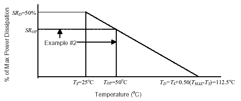
Figure 4: Transistor Derating Requirements, Example #2.
Operating temperature is 50oC. This is between
Top (25oC) and Ts (125oC), so the
center equation is used. Substituting,
The stress ratio allowed by the derating guidelines at an ambient
temperature of 50oC is therefore 35.7% of the maximum power rating.
Since the maximum power rating was given at 200 mW, the transistor is not
allowed in an application where it dissipates more than 71.4 mW. Since its
actual power dissipation was given at 70 mW, the transistor meets the derating
guidelines.
Alternative Solution:
An alternate method of determining if the transistor exceeds its
derating guidelines is to determine if actual junction temperature exceeds
derated junction temperature.
Actual junction temperature is calculated using the thermal
resistance properties of the device. The datasheet gave the thermal resistance,
junction to ambient (QJA),
as 0.875oC/mW. We also know the transistor is dissipating 70mW of
power. Junction temperature can therefore be calculated using the equation:
Substituting:

The derated junction temperature was previously calculated in Eq-4
to be 112.5oC. Since actual junction temperature does not exceed
maximum derated junction temperature, the transistor is acceptable to use in the
given application.
Note: the reason this short cut can be used is because the slope
of the derating lines in both Figure 3 and Figure 4 is equal to the inverse of the thermal
resistance. In other words, the junction temperature at any point along the
derating line will be the same.
Documenting The Stress Analysis
The next step in the electrical stress derating analysis process
is to calculate the stress ratios and document the results of the stress
analysis. The stress ratio is the numeric ratio between the actual stresses
determined from the circuit analysis divided by the stress rating of the part at
the operating temperature. This can be expressed mathematically as a percentage
as follows:
The best method to document a stress analysis is usually through a
worksheet or spreadsheet that allows for a logical flow of information from left
to right with all required data and parameters specifically called out in
columns. This obviates the casual omission of required parameters. the analysis
is most effectively accomplished with the use of different worksheets for the
various part categories. Many facilities perform the stress analysis, derating
analysis, and reliability prediction all in a single spreadsheet to increase
efficiency. It is also possible to generate macros to perform much of the
repetitive work. Examples of typical worksheets are contained in the following
pages containing Tables 1 through 6.
| |
Equipment |
Schematic No.
Rev
Title: |
Max
Alt:
(ft)
|
Next Assy
No.
Title: |
Ref
Des
(type) |
Const-
Struction |
Type |
Vendor |
Procur
Doc |
Nom
Resist |
Mfg
Tol |
TA |
Voltage |
Power Dissipation |
Percent
Power
Rated |
Percent
Voltage
Rated |
Wave
Form
(dc,
sine,
pulse, etc) |
Remarks |
Resistive
Element |
Nom
Rated |
Actual |
Rated
25oC |
Rated
Max
Amp |
Actual |
| |
|
|
|
|
W |
% |
oC |
V |
V |
mW |
mW |
mW |
% |
V |
|
|
| |
|
|
|
|
|
|
|
|
|
|
|
|
|
|
|
|
| Report
Number |
Rev
Date |
Proj
Appd Date |
Appd
Date |
Project No. |
Sheet
____ of ____ |
Table 1: Part Usage and Applied Stress
Data Chart for Resistors.
| |
Equipment |
Schematic No.
Rev
Title: |
Max
Alt:
(ft)
|
Next Assy
No.
Title: |
Ref
Des
# |
Const
Dielec-
tric |
Cap
Type |
Vendor |
Procur
Doc |
Part
Amb
Temp |
Cap
Value |
Mfg
Tol |
Voltage |
%
Volt
Rating |
Wave
Form
(dc,
sine,
pulse, etc) |
Remarks |
| Rated |
Operating |
| 25oC |
TD |
DC |
Peak |
AC
RMS |
Freq
|
Pulse
Peak
|
Rep
Rate
|
| |
|
|
|
|
oC |
nF |
% |
V |
V |
VDC |
V |
V |
KHz |
V |
ms |
% |
|
|
| |
|
|
|
|
|
|
|
|
|
|
|
|
|
|
|
|
|
|
| Report
Number |
Rev
Date |
Proj
Appd Date |
Appd
Date |
Project No. |
Sheet
____ of ____ |
Table 2: Part Usage and Applied Stress
Data Chart for Capacitors.
| |
Equipment |
Schematic
Title: |
No.
Rev |
Max
Alt:
(ft)
|
|
Next
Assy
Title: |
No. |
Ref
Des
# |
Vendor
Part
# |
Vend |
Procur
Doc |
Type
GP,
Power,
etc.
|
Part
Amb Temp
|
Contact
Arrage-
ment
(form) |
Contact Loading |
Coil
Voltage |
%
Cont
Power
Rating |
%
Cont
Curr
Rating |
%
Coil
Max
Volt
Rating |
%
Coil
Pick
Volt |
%
Coil
Drop
Volt |
Con-
tact |
Power |
Current |
Load |
Maximum |
Pickup |
Dropout |
Nom
Rated |
Act |
Nom
Rated |
Act |
Rated |
Act |
res/ind
cap |
Nom
Rated |
Act |
Rated |
Act |
Nom
Rated |
Act |
| |
|
|
|
|
oC |
oC |
|
|
mW |
mW |
mA |
mA |
|
mV |
mV |
mV |
mV |
mV |
mV |
%
|
%
|
% |
% |
% |
| |
|
|
|
|
|
|
|
|
|
|
|
|
|
|
|
|
|
|
|
|
|
|
|
|
| Report
Number |
Rev
Date |
Proj
Appd Date |
Appd
Date |
Project No. |
Sheet
____ of ____ |
Table 3: Part Usage and Applied Stress
Data Chart for Relays.
| |
Equipment |
Schematic No.
Rev
Title: |
Max
Alt:
(ft)
|
Next Assy
No.
Title: |
Ref
Des
# |
Vendor
Part
# |
Vendor |
Procur
Doc |
Type
Si
Ge |
Max
Amb
Temp |
Voltage |
Peak
Inverse
Voltage |
Forward
Current |
Percent
Current Rating |
Percent
PIV Rating |
Q |
TJ |
Notes |
Rated
25oC |
Rated
Max
Ambient |
Actual |
Max
Rated |
Actual |
Max
Rated |
Actual |
| |
|
|
|
|
oC |
V |
V |
V |
V |
V |
mA |
mA |
% |
% |
oC/W |
oC |
|
| |
|
|
|
|
|
|
|
|
|
|
|
|
|
|
|
|
|
| Report
Number |
Rev
Date |
Proj
Appd Date |
Appd
Date |
Project No.
|
Sheet
____ of ____ |
Table 4: Part Usage and Applied Stress
Data Chart for Zener Diodes.
| |
Equipment |
Schematic No.
Rev
Title: |
Max
Alt:
(ft)
|
Next Assy
No.
Title: |
Ref
Des
(type) |
Vendor
Part
# |
Vendor |
Procur
Doc |
Type
Si
Ge |
Max
Amb
Temp |
Power
Dissipation |
Peak
Inverse
Voltage |
Forward
Current |
Percent
Current
Rating |
Percent
PIV
Rated |
Remarks |
Rated
24oC |
Rated
Max
Ambient |
Actual |
Max
Rated |
Actual |
Max
Rated |
Actual |
| |
|
|
|
|
oC |
mW |
mW |
mW |
V |
V |
A |
A |
% |
% |
|
| |
|
|
|
|
|
|
|
|
|
|
|
|
|
|
|
| Report
Number |
Rev
Date |
Proj
Appd Date |
Appd
Date |
Project No. |
Sheet
____ of ____ |
Table 5: Part Usage and Applied Stress
Chart for General Purpose and Power Rectifier Diodes.
| |
Equipment |
Schematic
Title: |
No.
Rev |
Max
Alt:
(ft)
|
|
Next Assy
Title:
|
No. |
Ref
Des
# |
Vendor
Part
# |
Vend |
Proc
Doc |
Part
Amb
Temp
|
Power
Dissipation |
Voltage |
Current |
Perc
Output
Rating
|
Perc
Supply
Rating |
Perc
Current
Rating |
Perc
lc
Rating |
Q
Res |
TJ |
| Rated |
Actual |
Input |
Output |
Supply |
Collector |
Perc
Input
Rating |
@
25oC |
@
TD |
| Rated |
Act |
Rated |
Act |
Rated |
Act |
Rated |
Act |
| |
|
|
|
oC |
mW |
mW |
mW |
V
|
V |
V |
V |
V |
V |
mA |
mA |
% |
% |
% |
%
|
%
|
oC/W |
(oC)
|
| |
|
|
|
|
|
|
|
|
|
|
|
|
|
|
|
|
|
|
|
|
|
|
| Report
Number |
Rev
Date |
Proj
Appd Date |
Appd
Date |
Project No. |
Sheet
____ of ____ |
Table 6: Part Usage and Applied Stress
Data Chart for Linear
Microcircuits