Download the PDF file
Dr. Lawrence W. Kessler developed the acoustic
microscopy, non-destructive inspection technique at the Zenith Radio
Corporation, and in 1973, he acquired patent rights to form the Sonoscan Inc.
The original effort at Zenith was prompted by a need to screen for defects in
Plastic Encapsulated Microcircuits (PEMs) to alleviate a rash of warranty return
failures found to be primarily from voids at the die attach interface, and
de-laminations in the epoxy encapsulate at the package to die/lead-frame
interface(s).
Since 1974, Sonoscan has developed a variety of acoustic
inspection instrument models and techniques to aid the microelectronics industry
in developing and manufacturing plastic packaging (PEMs). This non-destructive
inspection technique is useful in both PEM screening and reliability assessment
of PEM product. Acoustic Microscopy Inspection is limited only to the material
thickness and acoustic transmission characteristic.
The most widely used technique is the C-Mode whereby a
device(s) can be inspected as if "mechanically" cross-sectioned. Slices of
variable thickness are made at desirable interfaces e.g., the package to die,
die to die paddle (die attach), and package to lead-frame. Anomalies and
discrepancies are readily detected by observing the echo signal characteristics
at the interface of interest. Anomalies and/or defects can be viewed as a
"looking-down-thru" image of the slice on the Sonoscan image display screen.
Also, the image can be presented as a printout for use in reporting.
A trained operator can detect
anomalies and defects in both the construction and material of the device being
inspected. The common anomalies and defects are voids, de-laminations, poor die
attach, poor adhesion at interfaces, excessive porosity, cracks in the package
and die, die misplacement and chipped die. Post environmental inspections will
detect variations and changes in material characteristics by observing changes
in the material grain structure. High temperatures typically cause surface
oxidation, which is detected by a significant loss of echo signal strength.
While the inspection of PEMs internal integrity is most
widely used, inspections of other product defects and anomalies are also
performed when non-destructive inspection and/or cross sectioning is required or
desired. Some examples of ceramic, metal and plastics:
Solder Coatings - poor adhesion (cause of future
flaking)
Surface
Plating -
inconsistent thickness, poor adhesion (potential bleed thru and
oxidation)
Surface
Quality (Ceramic/Glass epoxy) - mottling, porosity,
oxidation, layer de-lamination
Surface Quality (Metals/Alloys) -
scaling, pitting, corrosion (typically oxidation by oxygen & sulfur)
Material
Integrity (Resins, Epoxies, metals, alloys, ceramics)
- porosity, in-consistent density, internal fissures/cracks, blowholes,
inclusions
Bonding
Integrity (joints) -
Anomalies in welds (Cracks/voids/inclusions) and adhesives (coverage/thickness/degree of adhesion)
Acoustic Microscopy Theory & Operating
Procedure
I. THE "C-SAM"
PRINCIPLE
This system uses
transmitted acoustic signals and detection of the signal reflections - "echoes".
The signal is transmitted through DI water (alcohol or mineral oil may used as
well) into a solid sample, which may have one or more interfaces and may
contain several elements throughout the sample. It is the differences in
acoustic impedance between interfacing materials, which result in theses
echoes.
Transducer
frequency is chosen for the type of sample being tested. Thick samples usually
require a lower frequency transducer than thin samples because lower frequencies
provide better penetration. Higher frequency transducers provide the best
resolution for imaging details and locating thin interfaces. The frequency range
in this system is from 5 MHz to 150 MHz; however, higher frequencies are now
available.
NOTE: Typical
values of acoustical velocity "V" and impedance "Z" for the most frequently
encountered materials:
|
MATERIAL
|
ACOUSTICAL V/Z (V = km/S)
|
| Al |
6/17 |
| Au |
3/63 |
| Ag |
3.6/38 |
| Al2O3 |
10/35 |
| Epoxy Resin |
2.5/3 |
| H2O |
1.5/1.5 |
| W |
5.4/104 |
| Air |
zero/infinite (in this
system) |
The acoustic
signal is focused at a depth dependent on the sample construction and the
desired interface or element location (Target). When the transducer is focused
to a specific interface or element, a maximum signal is detected and appears as
a peak on the A-SCAN oscilloscope display; but, its amplitude is dependent upon
the properties of the material, the thickness of the material, and its clarity
may be affected by interfering echoes from elements and interfaces located
primarily above the desired target.
The amplitude,
polarity and time location of the focused peak signal display are all dependent
on the medium material and the distance the signal must travel. Focused
signals going from a very low resistance to a very high resistance and vice
versa will produce a relatively large echo (Large peak on the "A" scope). Echoes
from voids in the sample always produce large negative peaks on the "A"
scope display. The deeper the target, the longer the time for the peak
display.
The result of a
typically focused system in the C-SAM mode produces a discernable primary peak
and multiple secondary peaks appearing at different times along the oscilloscope
display baseline ("A" Scope, Channel 1 in this system). This is because
reflections can occur from interfaces (material differences or elements) that
are located above and below the focused target interface. Since these are not
focused they are usually reduced in amplitude, and ones closer to the surface
will be observed on this baseline before the desired peak. Signals also
penetrate deeper than the target interface and peaks may occur for each
interface encountered - but usually at reduced amplitudes and
significantly longer display times.
When a void or
de-lamination consisting of air or a vacuum is encountered, the signal travel is
stopped at that point; therefore, no interface or element can be inspected when
located directly below a void or a complete de-lamination.
Note: Should a
void or de-lamination cavity become filled with water, the anomaly will seem to
have disappeared. A bake-out at 60°C for ~
4 hours is recommended after a device has been subjected to any significant high
humidity environment.
A gate ("A" Scope
- Channel 2 in this system) is used to reduce the number of unwanted peaks which
might appear in the Video image display - the image generated at the end
of the analysis cycle. The gate is placed at the display time (depth) of the
desired peak from the focused targeted interface, and it's width is dependent on
the width of the desired peak, e.g. for PEM inspection: die only, lead frame
only, or die and lead frame together - the gate width is determined by operator
tailoring while observing the "A" Scope display.
Samples with
several interfaces of interest and elements (e.g. MCMs & ceramic capacitors)
are more difficult to analyze. As mentioned earlier, a sample with a separation
between layers or a cavity, cannot be analyzed through the separation layer or a
cavity. It is often necessary to analyze such a sample from both directions.
Several layers of different materials create
troublesome multiple echoes, which can make depth determinations of
interfaces difficult.
II. TYPICAL MODES OF
OPERATION FOR PEM ASSCESSMENTS:
A-SCAN - provides an oscilloscope display ("A" Scope) of vertical line information
thru the depth of the sample at a predetermined point on the surface. It
displays peaks at interfaces occurring at times proportional to their depth.
C-SAM - provides a video image display of a
horizontal cross section of the sample at predetermined depth at which the
transducer is focused and the gate is located. The image can be printed and/or
stored on the hard drive or on the Floppy
Diskette.
III. PEM ASSESSMENT CHECK LIST FOR ACOUSTIC MICROSCOPY
INSPECTION
1. Consistent internal construction (FIGURES 1 &
2)
2. Consistent die size & die placement (FIGURES 1
&2)
3. Consistent encapsulant material (Visual & Gain
variations) (FIGURE 3)
4. Package & die integrity (Cracks & chips)
(FIGURE 4)
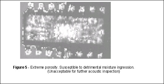
5. Porosity
(FIGURE 5)
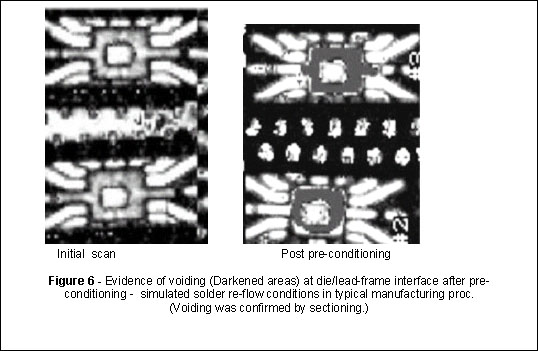
6. Voiding (FIGURE 6)
7. Adhesion (encapsulant-to-die/leadframe) (FIGURE 7)
8. Die attach (FIGURES 1 & 8)
9. De-laminations (FIGURE 9)
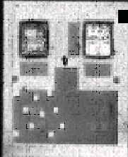
10. Unusual anomalies (FIGURE 10)
ACOUSTIC MICROSCOPY INSPECTION 10 POINT
CHECK IMAGES OF TYPICAL ANOMALIES
|
|
|
|
Initial Scan
|
Post
HAST
|
|
|
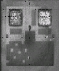
Figure 9 -
Multi-layered
device incurred de-lamination damage after 50 hours of HAST.
(De-lamination
was confirmed by sectioning.)
|
|
|
|
|
|
Initial
Scan
|
Post
HAST
|
|
|
Figure 10 - Multi-layered device with evidence of
oxidation damage after 100 hours of HAST.
(Echo
signal strength greatly reduced by oxidation results in darkened
image)
|
IV. SIMPLIFIED PROCEDURE
SONOSCAN
MODEL DAC244, CSAM MODE
|
TRANSDUCER & SAMPLE COMPARTMENT
|
MAIN DISPLAY
|
C-SAM
IMAGE
|
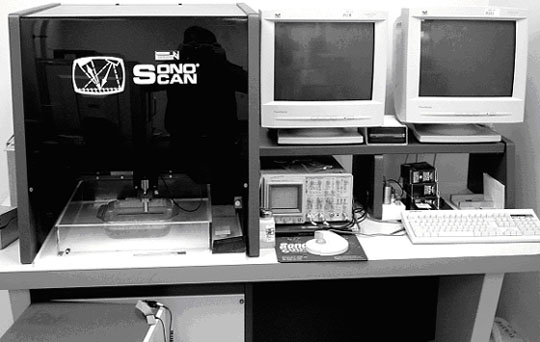 |
|

|
|
Power "ON" / "OFF"
Switches
|
1. Replace
de-ionized water if over 1 week old.
NOTE: Be sure
there is no "FLOPPY DISC" in the computer compartment.
2. Push green
switch located under console...turns unit on (red switch turns it off).
Log on and select, "VISUAL ACOUSTICS"
and follow the window prompts.
3.The system
automatically sets the X-Y axis limits...this takes a couple of
minutes.
4. "A" scope
Channel 1 is the main signal trace, 2 is the "GATE" trace, and Channel 3 is the
Trigger input - setup as follows:
4.1 Channels 1
& 2: 500 mV, sweep at 200 nS ("A" scope displays), and "DC" ("A" scope
panel).
4.2 Trigger on
channel 3 at "Auto", "+", and "DC" ("A" scope panel).
NOTE: This scope will shut off the display after
several minutes of inactivity...push "Beam Find" button to re-activate. Also, if
the "SETUP/AUTO" button ("A" scope panel) is inadvertently pushed, it will
change the sweep and trigger settings - re-set to 4.1 & 4.2 conditions.
5. The main screen
displays two "RF SLICES" - which provides the opportunity to scan two levels of
penetration with a single scan, however only the selected "RF SLICE" will appear
at the separate C-SAM image display monitor. Both "RF SLICES" will always appear
on main display (reduced in size).
6. Activate the
desired channel to be used and filed. Both channels may be used and filed.
7. Select the Scan
Size & Speed... initially, use a size to just cover the sample package and a
maximum allowable speed (usually 8 inches per second).
NOTE: When the
scan size is less than 20, the maximum speed is limited to 4 inches per second.
Also, for very small samples a slow scan speed is recommended to prevent
movement of the lighter samples which will produce a blurred
image.
7.2 If necessary,
install the appropriate transducer (available frequencies are 10, 15, 20, 30,
100 , & 150 MHz). Use higher Frequencies when observing details of small
sample areas. Use lower frequencies for thick materials to achieve greater
penetration. Set the proper transducer frequency...it is displayed on the
picture of the transducer at left of the main screen.
7.3 Set the
channel 1 (Main sweep) "GAIN" to around 35/55 DB and channel 2 to 25 DB (Gate
sweep) using the mouse at the "GAIN" locations in the main display. The total
available "SIGNAL" gain is 95 DB, but ringing can occur with excessive gains -
typical gains are 25DB (Channel 1) and up to 63.5DB (Channel 2). The gain is
normally adjusted to achieve the best image during the initial scans, but needs
to be tailored for the final displays to achieve the best image for
printouts.
8. Place the
sample into the water tank under the transducer. Place the mouse arrow on the
"UP" or "DOWN" arrow displayed at the transducer picture. Lower and raise the
transducer with the mouse buttons. Then lower the transducer into the water
about 1/2 inch Do not allow the transducer to hit the sample. Probe under the
transducer with a finger to remove any trapped bubbles.
NOTE: It is
imperative to remove all traces of bubbles. Also, the sample should be as
level as possible to keep the interface planes in focus during scanning...this
is significant with large samples or when scanning a group of samples at one
time - a variation greater than 0.2 uS in " TOF" can change the required gate
position and gain setting significantly.
9. Set the trigger
level to 1.000. The gain of the transducer may require tailoring and the "A"
scope settings may also require tailoring or re-setting to obtain a usable
display of the peak. The words "NO ECHO" will change to a number ("TOF") when
the transducer is over the sample and there is no bubble under the transducer to
block the signal.
10. Center the
transducer over the sample visually by using the mouse in transducer location
window in the main display.
11. Place the mouse curser on the "UP" or "DOWN"
arrow displayed in the "TOF" window. Lower and raise the transducer with the
mouse buttons to find the position of maximum peak amplitude of the first
peak found on the "A" scope display...this would be the point where the 1st
interface is in focus. Adjust transducer slowly (using the middle mouse
button) to confirm it is at the maximum peak. This will be the top of the sample
(or bottom, for up-side-down sample analysis). Using the mouse place the gate at the start of the channel 2 "A"
sweep - a gate width of 0.2 uS or slightly wider is recommended.
12. A C-SAM may
now be made to verify this by placing the mouse arrow on the "START " box and
activating the C-SAM with the mouse button. The gain will probably need
tailoring during the scan to achieve the best image. After the image is
displayed, center the transducer cursers using the mouse at the "X-Y" movement
matrix window - then "HOME" to establish transducer at the center of the
sample.
NOTE: There are
several choices to enhance the video image with combinations of "MAP" colors or
black & white; begin with Map "2"...it is usually best for the initial scan,
and it is normally the best for most samples. Map 24 is usually used to enhance
voids or de-laminations found in PEMs. The map choice can be made and changed
during the scan with the mouse. Other color maps are available for enhancement
of images, as required, to be used in published reports.
13. To locate
other interfaces, estimate the time it may take (TOF) to reach the wanted
interface and return to the transducer. Set the gate width to approximately 0.2
uS initially. Move the gate on channel 2 of the "A" scope to the expected
location of the "A" scope (CHANNEL 1), then lower the transducer while observing
both "A" scope channel displays. It may be necessary to tailor the system gain,
gate width, and "A" scope settings to see very small peaks.
14. When a peak is
observed, optimize the scope sweep time and sensitivities...it may be necessary
again, to tailor the systems gain and gate settings. If near maximum gain is
required, be sure the focus is not at an echo of the desired interface. Then
focus the transducer for maximum peak (raise & lower with the mouse at "UP"
& "DOWN" arrows) tailoring the gate position and width to select the wanted
peak.
15. When a peak is
at maximum, and fairly well isolated by the tailored gate width, initiate a
"C-SAM".
16. Repeat steps
12-15 until a quality image of the wanted interface is obtained on the "C-SAM"
display.
NOTE: As
mention earlier, if near maximum gain is required, be sure the focus is not at
an echo of the desired interface.
17. To retain and
document the "C-SAM" analysis of the sample, the image can be given a file
name/number, stored; and, also labeled with text, and ultimately
printed.
17.1 To save the image, access
the desired "IMAGES " files of the main display using the mouse, then select
"SAVE". Then create a file name for the
sample and enter it.
17.2 To save the image on the
floppy disc, same as 17.1 access "Convert Image" and select the file name. Then
enter it into the "TIFF" format. Both files ("TIFF" and the standard image file) will appear in the main
directory. Access the main directory and
select the "TIFF" file - then drag it into the "A" file.
17.3 To label the image to
appear on filed images, use the mouse to access "ADD TEXT". Locate the text area with the curser and type the desired label with the
keyboard - be sure to press enter at the conclusion of each line or end of
text.
17.4 To printout the image, be
sure the image is the best attainable quality (tailor the gain and map) and
labeled for sample identification.
V. APPLICATION EXAMPLES
NSWC-Crane has
examined PEMs, MCMs, ceramic capacitors, and a variety of samples. Comments
follow:
PEMs:
The set-up used the 15
and 20, and 30 MHz transducers to obtain required penetration for imaging the
die, die attach and lead frame. Map # 2, at moderate gains provided a good image
for highlighting voids (shows up as red in color map # 24). The peak at the
first interface was easy to find. Focusing on the die and lead-frame interfaces
and obtaining good C-SCAN images was also relatively simple.
MCMs:
Some problems were
encountered as these were a cavity device. It was necessary to analyze them
bottom up to avoid the cavity. The sample was a ceramic package with a ceramic
substrate epoxy cemented to the package. Die and other elements were mounted on
the substrate. A 100 MHz transducer and MAP # 1 (Black & White images) were
chosen; The 100MHZ transducer presented some penetration difficulties.
A C-SAM image of the
bottoms revealed the hand written sample numbers on each device. The stamped
part number also showed on most samples when imaging the bottom. The 1st
interface (bottom) was easy to find. In some cases the hand written sample
numbers were visible in the image scanned at the interface level. It would best
to avoid this labeling practice.
The epoxy interface
presented some difficulty as peaks could be found at two places close together
on the "A" Scope display. the 3rd peak was decided on as it produced the best
epoxy-to-substrate interface image. It was not possible to obtain an image of
the element/substrate interface with this transducer. The 30 MHz transducer was
tried but it was very difficult to isolate the two epoxy interface peaks, and
not much benefit was gained in penetration.
The entire group
of 35 samples was analyzed with the 100 MHz
transducer and good images of the epoxy interface were obtained.
Two significantly
different interface images were found. About half appeared to be a smooth layer
of epoxy and half were mottled in appearance indicating less than 100% coverage.
This could be a problem in dissipating heat during operation.
CERAMIC
CAPACITORS:
Ten ceramic
capacitors, containing 47 inter-digitated plates, were analyzed using the 15 MHz
transducer, by first finding the top interface, then the bottom interface and
setting the transducer focus midway between them. Using a wide gate and MAP # 1 (Black &
White images) produced a good image and showed de-laminations on three of the
ten samples. However, it was discovered that the samples must be scanned from
both the top and bottom to see all of the de-laminations that occur much closer
to one surface than the other.
Heatsink -
Al2O3/Al SUBSTRATE:
This assembly consisted
of ALUMINA/EPOXY/ALUMINUM/EPOXY/ALUMINA fabricated in alternate layers,
approximately in thickness of .060/.005/.125/.005/.060 inches respectively.
Interest was in the alumina-to-epoxy/epoxy-to-aluminum
interfaces.
Both the 100MHz and 30
MHz transducers were used with some success. The epoxy interfaces were located
and no voids or de-lamination were detected (Echoes from voids would have
produced large negative peaks). It was
necessary to scan from both sides to reach both epoxy interfaces. Calculating
the gate position of the epoxy was helpful and made possible by the material and
dimensional information provided with the sample. The 100 MHz transducer
provided the better image of the pattern found at the epoxy-to-aluminum
interface (a very narrow gate was used after locating the interface).