Recently, NSWC Crane was approached
to help perform failure analysis, fault determination and isolation on laser
damaged interline transfer Charge Coupled Devices (CCDs). The initial task
objective was to understand device construction/operation and determine which
laser-induced defects generate various failure modes viewed on the video output
of the CCD. Better understanding of CCD chip structure and operation, as well
as its failure modes, should facilitate better laser hardening
techniques.
After considerable effort was spent
acquiring data and information on device structure and operation, fault sites
that caused various failure modes on the CCD output were analyzed. The failure
modes included, but were not limited to the following:
Black
Spots
White Spots
Colored spots
Horizontal Black Lines
Vertical
White Lines
Blooming Cross-Like White Spot
Waterfall Effect
Half Blank
Screen
Blank Screen
Upon completion of both construction
and fault site analysis on numerous CCDs, theories were developed for various
chip behaviors observed after damage by a laser beam. Simulations were then
developed and tested to verify findings.
The intent of this document is to provide the reader with an
understanding of the work accomplished in support of this effort and provide the
insight necessary to introduce new and better laser hardening techniques.
Chip-level Basics of Failure
Analysis
This section will discuss the
process steps and techniques that are utilized while performing failure analysis
on Charge Coupled Devices (CCDs). The processes and techniques are discussed
below in typical order that they are undertaken during failure analysis. The
intent of this section is to provide information to the reader that will allow a
better understanding of the problem solving
process.
Review of Background Data
Associated with Anomalous CCDs
The
history and data of what has been done to a given CCD is thoroughly reviewed and
addressed. This includes the number and location of laser shots, energy and
frequency range, video image output of the device after each shot, as well as
other conditions related to the shots or response of the component.
All related
data, whether jpgs, gifs, Excel files, observations, etc, are reviewed together
with the electrical specifications related to a given CCD, so that the exact
state and behavior of the device is known and can be confirmed before failure
analysis begins. If the unit were fully functional, then a review of the
specifications would usually be adequate before proceeding with construction
analysis, simulation of failures and
deprocessing.
Capture Video Output of Operating CCD
During this step of the failure
analysis process, the unit is connected to power and its output is monitored via
a video recorder in order to observe the unit’s response to given laser damage.
When possible, this is done with the lens in place,
to help orient the video of the damaged area to the physical location of
the damage on the die surface. Light intensity is varied from zero light to bright light to record changes in video output at the location of
damage. Depending on the output and the behavior of
the CCD, the same operation is accomplished with or without the filter, and with
the use of fine focused microscope light or low power laser. This has
also proved to be beneficial in determining the exact failure modes of the
individual laser shots.
Package
opening
Generally, the cover glass needs to
be removed to complete the die inspection and photo documentation process and
also to de-process and identify depth and severity of the laser damaged areas.
Removal of the cover glass is accomplished by milling around the attached area
of the cover glass until breaching the package cavity. The cover glass is then
removed with a small probe or tweezers. The exposed device is cleaned with
alcohol, air and ultrasonic if needed. During this process, it is important to avoid disturbing
bond wires or permitting glass or package chips to damage the organic covered
array area. If removal of the cover glass is for the purpose of filling the cavity with fluid
and resealing, milling is continued until residual glass is removed and the
attachment area is smooth and level. The package is once again cleaned with
alcohol and air. The distance between the sidewalls of the package are measured
and a diamond saw is used to cut a new cover glass to replace the removed cover glass. Another opening method that has had
marginal success, is to plan sand through the cover glass until it is paper thin,
place inverted onto a piece of tape, and remove the unit from tape. The cover
glass should remain on the tape. During this technique, the CCD must be removed
from the board prior to sanding to avoid damaging the support components.
Debris has been the main problem with all opening techniques attempted to date,
with the sanding method being the cleanest, but also, the more tedious and difficult to complete. With relatively
small areas of laser damage, it is difficult to differentiate optically, even with the use of a wide variety of lighting methods,
between the mechanical damage from debris and laser damage. If possible, the damage sites are best identified and
documented prior to removal of the clear protective glass. There are several
variables that influence the quality of photomicrographs such as, damage size,
focal distance and lighting that can, under certain circumstances, make photo
documenting the damage unsuccessful.
Optical inspection
Optical macroscopic
inspection is utilized to correlate the laser shot damage to the video image output. For this step, it is important
to have as many details about shot locations and energies as possible. Locating and accurately identifying the
laser shots will allow for the photomicrographs of laser shots to be correctly
identified for comparison of the damage on the die surface to the failure mode
of the video output. All laser shots are photographed on a high variable power magnification microscope and overall
images of the CCD are photographed using low variable power microscopes. As with
the initial video output of the device, various lighting conditions, including
bright field, dark field, and polarization, are used to optimize inspection and
photographic documentation to maximize the information available from each site.
Electrical
Measurements
Volt-ohm
meter and curve tracer measurements are made on the pins of the device with and
without light. Testing on functional, nonfunctional, and damaged array CCDs has
not yielded much useful information. However, on-chip probing of undamaged and
damaged circuitry using a curve tracer or volt-ohm meter, especially after laser
isolation of portions of the circuitry, is instructive and useful. On chip
probing often assists in the understanding of the laser shot damage, whether it
be to poly-silicon gates, or more extensive and invasive
damage.
Probe/Laser Station
The laser station is utilized to
remove the topcoat on the die surface and allow access to the underlying
circuitry. Selected elements, metal or poly runs,
are then removed from the circuitry with the laser to simulate failure
modes and verify by electrical measurements
the different hypotheses for what conditions are present to cause the resulting
anomalous video outputs. This testing is performed while the device is under
power to allow monitoring of the video output during the isolation
process.
Component Preparation
Before cross section or angle lapping, the CCD device must
be removed from its board. The preferred technique is to use a low temperature
hot gas solder process to allow removal of the device being evaluated without
damaging surrounding components. There are circumstances that require the
device to be reinstalled on the board for further optical and functional
testing. This is accomplished with the same hot air flow soldering
process as removal. The isolation or damaging of
selected pixels in the array or other chip circuitry to simulate or duplicate
the behavior and damage that a CCD had upon receipt for failure analysis, can be
completed while the CCD is mounted on the board.
Package, Glass, Die,
Organic Identification, Removal & De-processing
Once all of the needed information
has been obtained from the CCD assembly and CCD device, the cover glass is
removed to allow further analysis by FTIR, SEM-EDS, and
Transmittance/Reflectance. Identification of the epoxy that holds the cover
glass can be identified by FTIR. Once the CCD chip-die has been removed, the
organics over the array can be identified by FTIR. Plasma etching, using O2,
has been found effective in removing the array’s cover coat, microlenses,
planarity layer, dyes, and other organics to expose the metallization,
polysilicon, and oxides above the silicon. The SEM-EDS can identify the
metallization and glasses used on the die. Normal chemical methods can then be
used to remove the insulating glass, metal, dielectric insulation, polysilicon,
etc, to gain access to the silicon surface.
SEM Inspection/Analysis
The areas identified and photographed
during optical inspections are typically submitted for SEM
analysis,
secondary, or backscatter, electron imaging,
Energy Dispersive Spectrometry (EDS), ‘point’ or area elemental spectra and
maps. Depending upon the depth and severity of the damage to the die, the SEM
photos give a much better image of the damage versus the optical
microphotographs. The SEM imaging, together with optical imaging, can also
provide indications as to the depth of the damage, whether surface, subsurface,
etc. The use of SEM-EDS permits the identification and elemental mapping of the
damage sites, which provides additional information about the cause of failure
or anomalous chip behavior. The SEM is
also utilized after beginning the cross sectioning. The sample can be
periodically viewed and documented during the entire sectioning process with much higher
resolutions than available with the optical microscopes, providing higher
magnification images, elemental identification and maps of the materials in the
areas of interest. The SEM inspections also provide additional information to
confirm or refine the theories of what has been damaged and why such damage
causes the chip to have the observed anomalous functional
behavior.
Cross Section, Angle Lap/Plan Section/Deprocessing/FIB/and
Staining
Cross sections of various types are very useful in confirming
and understanding the CCD circuitry, gate and cell array structure, and
composition. On a functional or damaged device, de-processing is accomplished
by utilizing a Plasma Etcher to remove the organic cover coat, lenses, planarity
and dye layers. Wet chemical processes can then continue the removal of glass,
metal, interlayer conductor glass, polysilicon gates, etc. down to the silicon
die. Cross sections perpendicular to or at a very slight angle with respect to
the side, just off the row and column line of the array will permit visibility
of the layers in-situ of the whole cell structure by moving along the section.
Staining of the silicon, which etches diffused, implanted, epitaxial and other
regions to a different degree, depending on the dopant impurity level, provides
visibility into the subsurface silicon structures. Perpendicular cross sections
at a 45 degree angle with respect to the array matrix can be used to provide
additional information on exact locations of the structures, particularly
damaged sites. For further clarification, a very shallow angle lap with respect
to the chip surface provides a magnification in the vertical direction and with
staining, can help clarify substructures. Inspection and documentation at
appropriate layers of each of the above sections or deprocessing levels by
optical, SEM, SEM-EDS spectra and elemental maps, permits complete understanding
of good and damaged areas. Due to its fine control compared to
mechanical-chemical sectioning, FIB sections of good and damaged areas provide
an additional, more refined view of the structures as needed.
Failure Analysis and Fault
Isolation
The
initial CCD was received in a nonfunctional condition. The device was subjected
to 10 laser shots of increasing energy, at an angle with respect to the surface
of the array. The entire die was inspected optically and photographed to
identify the array area, controlling poly silicon gates, parallel and serial
shift registers as well as the clock, gate drive, and power circuitry. An
electrical schematic was derived to help gain an understanding of the device’s
normal operation. This process also provides background information to assist in
exploring how the laser shots created a particular level of damage, either
causing local pixel malfunction, row or column problems, combined problems or
total device failure.
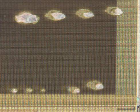
Image 1
High magnification photograph of the laser damaged
area.
The
chip was removed from its package and then divided in half via diamond sawing.
One half was utilized to successfully remove the organic cover-coat, lenses,
planarization, metallization, and insulating glass layers to gain access to the
underlying pixel structure. A portion of the other half was subjected to a very
shallow angle lap to clarify the gate interconnections and structure of the
array. Chemical staining of the pixel area was employed to highlight the
subsurface implants and silicon diffusions. The sample with the 10 laser shots
was cross-sectioned at 90 degrees successively into several of the laser shots
closest to the edge of the chip. Inspection of the laser damaged areas, both
optical and SEM provided additional information about the construction of the
array. The information obtained from the physical layout, optical and SEM
inspections, and SEM-EDS analyses permitted the reconstruction of the active
pixel area in the silicon array. Correct placement and alignment of the
polysilicon gates, light protecting metallization, dye and lenses confirmed
construction of the array elements.
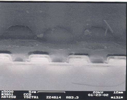
Image 2
Representative cross section of die
structure
The 90 degree
cross-sectioning process of the die was continued into the center of the final
laser shot which caused the device failure. Optical, SEM, and SEM-EDS analyses
of the sectioned unit in the area of the laser damage and outside the laser shot
area, where the device was undamaged, confirmed the hypothesized relationship
between the die structures and the pixel sketch showing that the device’s array
components were as expected.
In the area of the 10th shot, the
inspections confirmed that the clear coat, planarization layer, lenses, and
cover coat had been vaporized. The inspections and analyses also clarified that
the dual metal, aluminum over tungsten, light shield had been melted into the
polysilicon gates and into the silicon surface shorting the channel stops to the
pixels and possibly into the substrate beneath the epitaxial area. The melting
of the metal light shield into the silicon is shown on the SEM photomicrographs
and SEM-EDS and confirmed by the absence of metal above the polysilicon gates.
Damage exhibited at the failure site is typical of the extent of damage that is
sufficient to kill a semiconductor FET. Although no isolation or probe station
electrical measurements were made, the metal and polysilicon to substrate shorts
were clearly adequate to prevent device operation.
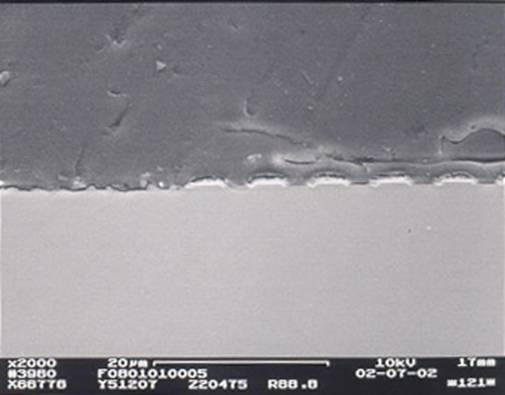
Image 3
Cross section of
laser damage
Inspection of the laser
shots from the top of the array and from the cross sections show the energy
distribution of the laser beam shots as they hit the array. The more significant
damage was at the center of the shot with less damage moving outward from the
center, reaching the edge of the beam where there has been essentially no damage
to the organics surrounding the laser shots. The cross section into the
5th laser shot shows vaporized and disturbed organics, but intact
metallization and polysilicon, confirming that the first 9 shots did not have
sufficient energy to melt the light shielding Al-W into the silicon, which would
cause complete disruption of functionality. The first 9 laser shots compromised
the pixels where the surface organics, dye, planarization layer, lenses and
cover coat had been removed or disturbed which would have eliminated the color
and light gathering ability of the affected pixels. However, as long as the
light shielding metal, polysilicon gates, and inter-metal/poly dielectrics
remained intact, the pixels not affected by disturbance or removal of the
organics would have (and had) continued to function normally, together with the
rest of the device.
FTIR spectroscopy was
used to identify that the array cover coat is acrylate polymethylmethlacrylatic,
and using subtraction techniques that the lenses and possibly planarization
layer, are Teflon based.
The cyan, magenta,
yellow, and green dye over the pixels beneath the lenses had insufficient
material to identify their composition. There was a test pattern of the
complimentary color and green dye matrix on metal, but the individual dyes were
the same size as those over the pixels, preventing the analysis of their
individual compositions. Complementary color dyes are used instead of primary
colors so that more light is available to the silicon’s pixel photon detectors
for increased sensitivity.
A second unit
received 36 laser shots of increasing energy in the nano/pico/femto second range. The induced damage was insufficient to
cause total failure of the device, allowing for a more detailed investigation of
the video output verses the level of damage to the die structure. The laser
shots were perpendicular to the surface of the die and had a very narrow
diameter, a few pixels, or in some instances, only a single pixel was
affected. Approximately 27 of the 36 shots were detectable by optical
microscopic inspection. However, the number of damage sites visible when
operating, varied from less than 27 to more than 27, depending upon the angle
and intensity of the applied light on the array.
Image 4
Optical microphotograph of laser shot
damage
Inspection of the damaged
spots using high magnification microscopes indicated that the laser had
disturbed either the dye, planarization layer, or micro-lens depending on the
shot energy of the damaged area inspected. With increasing energy, a
corresponding increase in the depth and severity of the disturbance was observed
in one or more of the layers. To observe the extent and location of damage it
was necessary to continuously vary the focus and mentally reconstruct what was
being seen into a three dimensional image. While small sections of
metallization could be seen on selected spots, there did not appear to be any
significant damage to the metallization.
With a
focusing lens attached to the CCD, the camera board produced a nearly normal
image, except at the small laser damaged areas. Different colors of light or
dark appeared, depending upon which pixels, how many pixels, the amount of dye
disturbed, and the amount of damage to the pixels’ micro-lens as well as the
interpolations of the camera board’s image (and pixel) adjusting algorithm
electronics.
A small
diameter light beam from a high magnification microscope that is co-axial with
the optical axis was slowly moved near the edge of the dim, dark, or colored
damaged spots. When the light was applied, the damaged spots would output a
light level corresponding to or exceeding that of the undamaged pixels around
the spots. This confirmed that the damage did not extend down into the
metallization, polysilicon, dielectric isolations, or silicon, where the light
was being ‘properly’ transformed into an electrical charge. Without the
addition of the higher intensity light, damage to the dye, planarization, and
lenses deflected, absorbed, or reflected the ‘normal’ light in which undamaged
pixel areas functioned correctly.
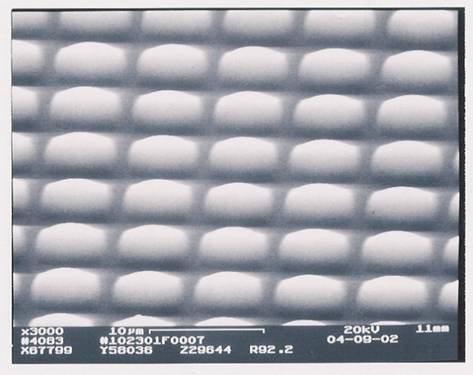
Image 5
SEM photo of laser
damaged area
Of interest at the laser
damaged spots, visible by optical or functional malfunction, was that SEM
secondary and backscatter electron images at various acceleration potentials and
at various magnifications were unable to detect any difference in the cover coat
or lens shape over the damaged spots compared to undamaged spots. This finding
together with the observations made above, confirmed that the damage or
disturbance was localized to the organics between the cover coat and the
dielectric layer covering the light shielding metallization and silicon. Even
the highest energy shot area was indistinguishable from fully functional pixel
areas.
A third unit was laser
shot 38 times with 24 of them optically visible. The range of energies was in
the nano/pico/femto realms. As with the previous units, varying the light type,
angle, shading, etc. caused some of the spots that were not operationally
visible to become visible. This suggests that the lower energy shots did
disturb the organics, but that light perpendicular to the array was not the
angle at which the light was attenuated the most.
The first 14 of the 38
shots did not output light when the unit was not illuminated. This was due to
the lower energy shots not causing damage down to the silicon, but instead the
damage was limited to the organics. In fact, there was so little damage on the
first 14 shots, that no evidence of damage could be detected on them with
extensive high magnification microscopic inspection in the exact locations of
the shots.
The next 24 shots did
exhibit light output, even when the unit was not illuminated. This was probably
due to the damage reaching the lower portions of the structure, including the
dielectric-silicon interface, causing charge injection, which the unit would
shift out even when under total dark conditions.
Comparisons of the last
24 shots show an increasing depth of damage and a slight increase in the number
of pixels involved. The light or absence of light output, from the damaged
areas, also relates to where on the pixel the highest energy of the laser pulse
struck, as well as the other factors previously mentioned during discussions of
other units.
The device did not
exhibit any of the horizontal black lines seen on the previous devices. The
main reason for the absence of the black lines is that these laser pulses have a
much tighter, narrower energy distribution so that the sides of the damaged
areas tend to be vertical rather than sloping as with the broader energy
pulses. These narrow laser beams tend to cut the polysilicon gates cleanly and
do not short them to adjacent layers of the light shielding metal or substrate,
compared to the shallow sided crater cuts with broader energy distributions
which were more likely to permit shorting of the polysilicon gates to adjacent
conductive layers, causing the horizontal black lines.
Inspection of the highest
energy shot 38, which is also the deepest as seen by comparison of damage
depths, indicated that the light shielding metal has melted into the silicon
substrate. The metal contact, as with the previous unit that exhibited column
blooming, caused the deposition of charge into the column, or columns, in excess
of what the gate voltages and electronic shutter could control.
Enlargement of the
operating unit’s image without light reveals the blooming column either had
several columns damaged by the laser shot or that the primary blooming column
has sufficient excessive charge to over-ride the channel stops’ voltage fields
and spill charge into adjacent columns, the left being blue-ish, the right being
white-ish. Of interest is that the adjacent columns do not have continuous
charge accumulation, along their columns. Rather, the blooming in the adjacent
columns appear to have every other pixel ‘light’ and the ones in between dark,
or normal. That phenomenon is most likely due to the way the CCD reads out
alternate fields, during which every other vertical pixel is kept ‘off’ by the
gate and the adjacent gate kept ‘on’ until the next field, after which, the
process is reversed.
The vertical transfer of
charge is from the bottom to the top of the screen in this image. Thus, the
enhancement of the blooming, greater light intensity, and color change of the
columns from blue-white-white to green-yellow-orange, is most likely due to a
build up of charge as the vertical control gate pump the charge to the
horizontal shift register together with affects due to the units control board
electronics. If it were due to damaged columns and channel stops, one would
expect the phenomenon to be at or near the damage site, which is causing the
problem.
Upon closer examination,
spots 24 through 38 also exhibit blooming into adjacent pixels but only on the
row(s) where the primary pixel damage has occurred. As with the whole column
blooming, the single or a few pixels, blooming is most likely due to a local
disturbance of the channel stops that lets the charge bleed over into the
adjacent column.
As with the other units,
operational behavior of the device with a focusing lens produces a normal image
over the whole array except in the damage spots and along the blooming
column(s).
A fourth device received
11 laser shots, spaced so that there was no overlapping of the rows or columns
affected by the damage. This was beneficial for the clarification of damage and
allowed for a more definitive failure analysis of the individual
shots.
Functional video images
from this device produced normal images except in the circular areas of the
laser damage. There were three exceptions to this general observation. One
shot has one or two dark rows extending from both sides of the spot and becoming
less dark the further from the center, until the rows appear the same as those
that were fully functional. The highest energy shot produced an essentially
identical dark line radiating from both sides of the center crater. In the area
of the dark horizontal lines, no video information was obtainable from the
related pixels when capturing an image, even though the dark lines did pass
information through the dark line. The dark horizontal lines relate to the
center of the craters where the highest energy and damage occurred. The damage
in the center of the two craters shorted the metallization to the underlying
polysilicon gates. Light striking the pixels associated with the dark lines was
still causing the generation of hole-electron pairs. However, because the
voltage on their related gates was shorted, the electrons were not stored and
those pixels appear dark, as if no photons had struck the photo detectors. The
relative high resistance of the polysilicon gates, compared to aluminum,
permitted the gates in the center of the laser craters to be ‘shorted’ by metal
yet because of their relative high resistance the polysilicon gates away from
the craters had sufficient voltage to store electrons from the photon generated
hole-electron pairs.
The bright vertical lines
originating from the highest energy laser shot, are caused by the vaporization,
melting and shorting of the metal light shielding mask through the dielectric
and into the silicon of the columns, bounded by channel stops, injecting charge
into the columns, causing blooming that masked any hole-electron pair generation
and storage in those pixels, preventing them from producing the image from these
areas.
The damage craters
related to the laser shots on this part exhibit an increasing amount of concave
ablation of organic material with the corresponding increase in laser energy.
This unit was also
examined using the IR microscope with negative results. However, when this part
was examined in the Emission microscope, three of the craters displayed light
emission because of the loss of some of the electrons’ energy as or after they
traversed the damaged oxide. This confirms that the shot had caused damage at
least down to the dielectric above the metal and silicon and probably into the
silicon. It is interesting to note that one shot did not exhibit any light
emission. However, the organic damage could be blocking areas where there are
oxide problems shown by the electron energy loss, in the form of light, or that
the crater in question did not experience the same severity of damage to the
oxide. It is also interesting that one crater did not exhibit either a black or
white line fault. But, that also can be explained by the probability that the
energy dissipated in the crater just happened to not involve either the
polysilicon gates nor the silicon columns in the same way that the shots did in
the other two craters.
Without further analysis,
isolation and measurement of the polysilicon gates to other structures, it would
be difficult to determine how many gates are involved in the dark lines and how
many columns are involved in the light blooming. A single column could be
involved, if it had sufficient charge or connection with the channel stops, or
several columns could be brighter because of the overflow of charge from the
primary column short into adjacent columns.
A fifth
unit had received 9 laser shots with energies from the nano/pico/femto realms.
When the camera is operated with ambient laboratory light, 2 to 4 of the spots
can be seen, depending upon the lighting or shading of the array. The visible
spots appear as colored dots of light, or dark spots. With a lens mounted to the
device, the rest of the array when in light is fully functional. During
operation in complete darkness, four or five of the nine spots were visible in
the video output.
Optical inspection of the
spots with both low and high magnification microscopes, show different amounts
of damage to a varying number of pixels, depending on the energy, time realm,
and exact location of the center of the laser shot with respect to the array
structure. The video image is affected differently depending upon whether the
laser strikes on metal between pixels beneath the lenses, or on the silicon and
dye coating, as well as the amount of energy and diameter of the laser beam.
Inspection of the remaining spots that did not produce functionally visible
anomalies, revealed no optically visible damage. The spots were visible in the
video output because the clear coat, lenses, planarization layer and/or dye, had
been disturbed sufficiently to cause the laser damage to adversely affect the
light path compared to undamaged pixels.
The fact that the
damage spots were also visible when the unit was functioned without any light
indicates that the laser damage had also disturbed the dielectric-silicon
interface or the slightly-sub-surface silicon, so that the damage caused
hole-electron pairs to be generated, the electrons accumulated, stored and read
out as if photons had impinged those spots.
Because the other 5 spots
could not be seen during functional operation, in light or dark environments,
nor by high magnification microscopic inspection indicates that those spots did
not incur sufficient damage to be detected by the device or its board
electronics reconstruction algorithm.
As with the previous
units, except the initial killed device, this unit could have polysilicon gates
related to the spots checked for resistive shorting by isolation, electrical
probing, and measurement related to other structures. This could be followed
by appropriate FIB sectioning and FIB-EDS to confirm the location and severity
of the damage caused by the laser shots.
A sixth
unit received 27 total laser shots with all shots in the nano/pico/femto realm.
Operation of the unit with lens showed ~12 shots of varying size and color.
Also seen were several adjacent vertical blooming columns that had minor
horizontal blooming, without an image, just at a given level of light. With no
light, the horizontal (left) ‘light’ blooming from the blooming column had two
overlapping areas, with the closer area being slightly brighter than the further
one.
Finally, a
most interesting blooming column(s) was observed that had an operational, image
producing section between its lower and upper blooming portions of the column.
This is the first column found that did not bloom its full length, preventing
any image production from that column. With this column, the bottom ¼ of the
column bloomed with a triple of different colored spots at its top. The next ~
1/3 of the column produced an image even thought the top 42% continued to
bloom. One would expect that with the top portion of the column blooming, which
is nearest to the horizontal serial readout shift register, that any signals
coming from the operational pixels (between the blooming column) that had to
‘pass through’ the blooming column to reach the output shift register would be
masked by the blooming of the column. However that is clearly not the case.
Initial
attempts to explain how this phenomenon could occur were frustrating and
frustrated. It caused a re-thinking of exactly how a CCD moved charge from its
array to its output and finally to the screen.
Because
one sees a constant image from the CCD-board-camera, an impression and
conclusion is easily, but mistakenly, made that the charge is not being read out
in frames with the electronic shutter acquiring photons for a fixed time
period. However, the reason the CCD does read an image from the middle
operative length between the column blooming at each end is that the blooming
has not consumed the column. There is a lesser charge level than fully blooming
columns, which permits the pixels in the middle between the blooming portions to
acquire photons/electrons/images normally. Once the electronic shutter ‘closes’
and photon/electron acquisition stops, the vertical shift registers move the
frame of pixels, row by row, into the horizontal shift register and output.
Thus, the operative pixels in the column do not really have to move through the
blooming column to reach the horizontal register and output.
What is
interesting, is how the signal from pixels on the opposite side of the
horizontal shift register read their signals out, the same mechanism is
operative. However, the more common full blooming columns had confused the
issue since they had sufficient damage and enough charge to overwhelm all of the
pixels in the column.
Several
additional anomalous phenomena were observed when watching the image produced
during CCD operation and light conditions varied with the view or the unit was
pointed at an even field of light that was then decreased till no light reached
the array. The fully blooming multiple columns had sufficient damage to spill
into adjacent columns and increase the length of blooming in the adjacent
columns with increased light intensity on the array. There was also a
translucent appearing lateral ‘waterfall’ to the left of those columns with
ambient light. However, with no light reaching the array the translucent
‘waterfall’ becomes much more visible, although it was still not bright and the
single one that was slightly visible in ambient light becomes two, one
overlapping the other.
A seventh unit received 9
laser shots in the nano/pico/femto realm. The 9th shot caused the
part to become non-functional. DC measurements on each of the failed CCD’s pins
yielded essentially the same values as the pins of a fully functional device.
The failed and fully functional CCD’s were removed from their control
electronics boards and switched to the other CCD’s board. The failed CCD
remained non-functional giving the same no output as it had on its initial
board. The units were returned to their own boards and again, as expected, the
failed CCD provided no output and the fully functional CCD again was fully
functional confirming that the control electronics were not involved in the
CCD’s failure.
Optical microscopic
inspection of the 9 shots confirmed that the damage on the CCD increased with
each increase in laser energy. High magnification inspection of the
5th shot showed that the spot had damage similar but greater in depth
than that of the last shot on T0002 which had vertical column blooming. SEM/SEM-EDS inspection of
previous damage on other failed parts indicated that the laser had vaporized the
organics and melted the light shielding metallization into the substrate as well
as melting the silicon photo detectors to the underlying silicon and channel
stops. The level of damage was sufficient to prevent the operation of the
device by essentially shorting the light shielding metallization, polysilicon
gates , photo detectors, substrate implant, P-well, P+ channel stops, and N
substrate which reduced on-chip voltages to ineffective/inoperative
levels.
Confirming the failure
and determining the exact cause of failure at spot 9 would be accomplished by
isolating the polysilicon gates related to the damage area, and electrically
microprobing from them and the light shielding metallization to the on-chip gate
outputs, on-board bias generator, substrate and power supplies. The DC voltage
levels of the failed and fully functional CCD pins indicate that the control
electronic board voltages were still functional. Complete verification that was
the case would be done by measuring the failed and functional CCD pins with an
oscilloscope with sufficient digital memory depth to confirm that the control
board electronics signal levels and waveforms were the same.
Further analysis that
would provide additional confirmation would be SEM, SEM-EDS spectra and
elemental maps of spot 5 and spot 4. And, FIB followed by organic plasma
etching, silicon decoration, and SEM, SEM-EDS of both ‘kill’ spot 5 and
‘non-kill’ spot 4, for comparison.
An eighth
part has 4 types of anomalies from the laser shots. It is interesting that all
16 shots can be seen on the video output of the device when the array receives
no light. And, that 11 to maybe 13 are visible when the device is operated in
the light. As with the previous units, variations in light and shading on the
operating device caused changes in the appearance of the spots and also caused
changes in the green waterfalls.
Several
of the types of damage have been seen and explained on previous devices. The 3
black horizontal lines, with a white line above and below the dark lines have
been previously discussed. Here, the damage is a bit more severe, covering a
greater number of gate sets, which most likely gives rise to the ‘bracketing’
white lines. Additional work will be necessary to properly address the cause of
the white lines. However, it could well be an artifact of the decoding
circuitry algorithm of the CCDs control board electronics.
The
16/11-13 (‘small’) spots down the left hand side of the device are related to
previous spot damage and the several different spots can be explained with a bit
of additional information. The vertically elongated spots with the unit under
both dark and light conditions are a bit different than the other spots on this
part and on previous parts. But, it is really a matter of degree. Here the
longer vertical spots have damaged more pixels vertically than previous damage
spots, thus, they appear as streaks instead of spots. Optical low and high
magnification microscopic inspection of the 5 greater elongated spots confirmed
that the laser damage with larger circular area at increased energy,
corresponded to the greater vertical, and horizontal, number of pixels that were
damaged, hence the length and width of the line.
Viewing
the video of the unit taken after the laser shots, with the filter in place, the
3 black lines appear white and there is a very narrow [probably a single column
instead of the multiple columns seen on the other units] vertical column
blooming from the 2nd large spot down to the bottom of the screen.
There is also a ‘split’ narrow [single column] blooming column associated with
the 5th large spot. Neither of the column bloomings were as clearly
seen when the unit was operated and its output recorded at Crane. The single
columns were occasionally visible, but just for a short time. Thus, the
lighting conditions, intensity, wavelength, angle, presence of filter, and lens
determined whether and how visible the two blooming columns were when the device
was operated.
An inspection of the
optical photomicrographs of laser shots numbered 1 and 5 indicate that the
damage to the device was from the light shielding metal melting down to the
substrate, or damage to the dielectric-silicon interface, silicon of adjacent
(vertical) pixels, and local damage to channel stops so charge could spill to
adjacent columns but only for a portion of the column.
The green ‘waterfalls’ do
not prevent images from ‘beneath’ them from reaching the horizontal serial
output register that is at the top of the image. That is clearly seen when the
unit was operated with the blue filter and focusing lens reinstalled on the
device and images of the lab were taken. The images in the green waterfalls are
blurry and somewhat distorted but can easily be recognized. And, with the unit
with blue filter and focusing lens removed, placed in a micro probe station and
a tungsten probe moved over the array into the second waterfall, again, the
probe is slightly blurry but easily seen. In both cases, whether views of the
lab and the position of the probe, the acquired image [pixel charges] of the
probe had to traverse the waterfalls and the dark row lines to reach the
horizontal output serial register, which is at the top of the image with its
output on the left, and visible on the video monitor.
The size of the damage
corresponded to the energy level of the laser shots. Thus, we are left to
explain the 5 ‘long’ vertical white-yellow-black outlined shots and the 3 green
waterfalls and should probably address the apparent discontinuities in the
bottom two black lines within several spots along the green
waterfalls.
-The
waterfall effect was created due to decreased gate voltages and stray
substrate.
-The charge transfer efficiency is decreased. However, pixels
within and outside the waterfall are receiving the same amount of
charge.
-Shorting
the gate or cover metal to the charge well caused white vertical lines, which
creates an overload of charge that the CCD cannot handle, thus the blooming
effect occurs.
-Notice that areas between the light lines were still
behaving properly due to channel stops remaining intact.
-Failure modes are typically a result of the depth of
damage caused by a specific laser shot and the laser’s exact location in a
pixel/group of pixels.
-The diameter, location, focus, and
energy of the laser beam are also critical.
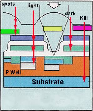
Figure
1
Figure 1 above highlights some of the locations/positions of the laser shot within a
pixel (or group of pixels) and which layers/surfaces are damaged or shorted to
the next underlying (or adjacent) layer cause the damage seen on the video
output.
Summary of Failure
Theories
Theories of
Failure
Once
the cell structure, array, chip schematic, on-chip circuitry, physical layout,
and drives/controls/algorithms/output controls from the PWB controller are
known, the video output of a functional and an anomalous CCDs response to light
and dark can be analyzed. Failure theories are established, refined, and confirmed by
looking at many different data streams, including, but not limited to the
following:
-Electrical measurements and characterization of the
device
-Visual
CCD-board output (video screen) responses to the laser shots
-Measured
and visual response to zero light, low through high level microscope and laser
light, etc.
-Knowledge
of laser spot size, shape, energy, time range, (and wavelength) per damage
site
-Understanding of individual damage sites via selected optical
microscope(s) and various mode and light exposures
-SEM
inspection, including SEM-EDS spectra and elemental maps,
-Layer by
layer deprocessing of the array
-Cross
sectioning of the various damage sites
-Shallow
angle lap with decoration/staining
-FIB
cross-sections in vertical, horizontal, and 45 degrees of characterized damage
and undamaged sites, if available
-Emission
microscopy of failure sites
-Scanning
capacitance probe
-Other analytical method outputs as appropriate
Literature,
seminal and other textbooks, manufacturer’s part data, university, and research
web sites and patent searches augmented CCD cell structures, lenses, circuitry,
and operation. Combined with the data listed above, failure hypotheses were
devised for the cause of the anomalous behavior. With the hypotheses and
theories thus devised, methods to test, refine, refute, or prove the theories
can be devised. Methods include duplication or simulation of the failure by
physical, mechanical microprobe, laser, light or chemical methods on functional
units.
Explanation of Chip
Failure due to the 10th shot
-SEM results showed that metal and
poly had been vaporized and melted to the substrate at the center of the damage
area.
-Extent of damage caused a low
resistance short of metal to the gates, the substrate implant (n-) and p- and p+
channel stops.
-The short pulls the gate voltages
down to ineffective and inoperative values.
-Shorting of the implants and
diffusions loads the power to the unit disturbing (lowering) their values and
preventing device operation.
-Vertical shift gates, horizontal and
output sense amplifiers are inoperative.
-Concentration of varying degrees of
light on laser spots causes dark spots to “disappear” on video
output.
-Indicates that damage is limited to
dye and lens material, not underlying glass/metal/gate structures.
Hypothesis: energy wavelength did
not disturb overcoat layer and instead damaged dye and lens material
underneath. The overcoat layer acts as a barrier to viewing damage when using
SEM.
Horizontal dark lines adjacent to and on each side of laser
spots 8 & 11
-Radiate along a gate or two for some
distance and are darker at the damage circle and lighten further away from the
damage area until normal function resumes as the operating voltage gets closer
to normal levels.
-The 4 phase poly gates are powered
from each end of the array and are individually continuous.
-Dark lines of the gate polysilicon
shorted at the damage circle run perpendicular to the channel stops and cross
some 30 to 50 channel stops (which define the vertical serial shift register
width and thus pixel width).
Explanation of dark lines on CCD output
-Laser energy melted metal to the
underlying poly gates causing a resistive short within the damage area (poly
gate is more resistive than aluminum).
-Thus, with applied power to both
ends of a resistively shorted gate(s), a variation in the dark line (darkest at
the damage circle) is expected.
-Can verify this theory by isolating
gates and performing curve tracer measurements from the 4 phase gates to ground
and the 3 power pins.
Explanation of lighted column
-Emission Microscope results indicate
that emitted light was at a higher level on spot 8 than any other spot (also hit
with the most laser energy).
-SEM photos indicate significant
metal damage (center of damage area - worse than other spots).
-Spot 8 also exhibited “dark line”
damage.
-Damage suggests that the metal and
poly gates have been melted into one or more of the vertical serial register
columns.
-Metal and gate(s) are making
electrical contact with the n- and p- (and probably p+) channel stops that
define the column(s).
-Voltage on the cover metal or gates
therefore is resistively shorted to the substrate in the affected vertical shift
registers defined by the channel stops.
-The cover metal or gate voltages cause charge injection in the
affected vertical shift registers at the damaged area so that the column’s pixel
signals all appear to have accumulated a significant amount of light greater
than the rest of the
array.