Download the PDF file
This section describes failure mechanisms and
anomalies of microcircuits. Use this section as a guide to design and select
microcircuits.
Failure Mechanisms - General
Microcircuit manufacturers have long since learned to
control and reduce failures in their wafer fabrication and hermetic package
processes. However, the plastic encapsulated microcircuit (PEM) processes are
still maturing with some problems still not controlled as well as users would
like. The military now allows the use of consumer, industrial and automotive
microcircuits in applications. Since PEMs are fairly new to the military, their
reliability and performance over time remain the subject of scrutiny by both the
manufacturers and users.
Consumer-grade PEMs are the riskiest microcircuit
products used by the military. The main areas of study regarding their use are
their unique failure mechanisms. Until studies are complete, designers should
continue to monitor these parts and not assume there is complete freedom to use
any microcircuit in any environment without concern for reliability. The risk
should be minimized and the parts should still be monitored. Both producers and
users in the military marketplace should know the potential failure mechanisms
and anomalies of each microcircuit they plan to use. Because of the newness and
risk PEMs place on the military industry, this section describes them in more
detail.
Figure 1shows recent failure mechanism breakdown data for packaged die at microcircuit
manufacturer facilities.
The Naval Surface Warfare Center, Crane Division has
been periodically assessing PEMs for over 25 years. For an example, they
recently assessed over 3,000 PEMs for Trident Fire Control, Trident Navigation,
CEC, Army Tank Command (TACOM), and the NAVSEA Parts Reliability and Derating
Manual Programs from 1997 through 1999. Figure 2
shows the number of failed, marginal, and passing PEMs during this assessment
period. The more common failures and anomalies found during this assessment are
(1) improper moisture-sensitivity-level of package, (2) contamination, (3) poor
die-paddle construction, (4) poor wire-bonds, (5) voiding, and (6)
delaminations. Having 30% of the total microcircuits either failing or being
marginal enforces the obvious need for PEM assessments and
monitoring.
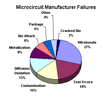
Figure 1. Microcircuit
Manufacturer Failures
Source: ICE, “Roadmaps of
Packaging Technology”
Figure 2. PEM Assessment
Results
Source: NSWC-Crane Division
Table 1 and Table 2 cites some of the more common microcircuit failure mechanisms and anomalies with
their probable causes.
|
Type
|
Example
|
Most Likely Cause
|
See Figure
|
|
Chemical
|
1. Corrosion
2. Contamination
3. Dendritic
Growth
4. Metal Migration
5. Intermetallics
6. Oxides
|
Moisture and Ionic.
Poor process control by
MFR.
Moisture, Bias, and exposed metal.
Current density in Al metallization.
Inter-reaction of dissimilar metals E.G. Al-Au
(Purple Plague).
Metal exposed to oxygen.
|
12
9
14
13
|
|
Physical
|
1. Open Circuit
2. Short Circuit
|
Loss of bond/wire integrity, or cracked die from
overstress by Thermal/Mechanical Shock, or Vibration, or weakened interconnects
from Bond misplacement and from Corrosion/Electro Migration. Loss/weakening of
wire-bonds from sweep during injection of molding compounds.
Particle or interconnect wire, metallic migration,
dendritic growth-poor process control.
|
6
|
|
Function
|
1. Loss or Degrade
|
Electrical Overstress, ESD, Radiation, High
Resistance Electrical Contact, High Temperature Exposure.
|
|
Table 1. Failure Mechanisms:
Die/Interconnects
Chemical Failure Mechanisms
Historic chemical failure mechanism concerns with
hermetic seal microcircuits also apply to PEMs; for example corrosion,
contamination, dendritic growth, metal migration, oxides and intermetallics.
PEMs are even more likely to develop "Purple Plague" because of the wide use of
Aluminum (Al) and Gold (Au) in their wire bond fabrication. Although PEM
manufacturers now use greatly improved encapsulant, additives such as bromide
(fire retardant) can introduce halogens which produce corrosion when combined
with moisture - all plastic encapsulates absorb moisture. PEM manufacturers now
use encapsulants with additives such as bromide (a fire retardant) which can
introduce halogens that produce corrosion when combined with moisture. All
plastic encapsulants absorb moisture and improperly cured encapsulants can
result in excessive porosity and moisture absorption.
Improperly cured encapsulant can result in excessive
porosity and moisture absorption.
|
Type
|
Example
|
Most Likely Cause
|
See Figure
|
|
Chemical
|
1. Corrosion
2. Porosity/Pin Holes
3. Solderability
4. Marking
|
Salt or Harsh Atmosphere.
Poor cure of Encapsulant by MFR. (Encapsulated IC);
Inferior grade of metal (Hermetic IC).
Poor finish by MFR. or Harsh Atmosphere.
High Temperature Exposure, Harsh Atmosphere or
Cleaning Agent.
|
10, 11
1, 15,
16
|
|
Physical
|
1. Leaks
2. Rupture -
“Pop Corning”
Delaminations
3. Lead Seal
|
Poor weld or braze by Mfr., Fatigue by Thermal/
Mechanical Shock or Vibration (Hermitic seal IC).
Absorbed moisture expands during solder operation
(Encapsulated Packages), poor process control, Thermal Shock (Encapsulated
Packages).
Poor process control of Lead/Package seal by MFR.,
Mechanical Fatigue from Vibration to Temperature Cycling. (Both Package
Technologies).
|
2, 3,
4, 5,
7,
8
|
Table 2. Failure Mechanisms:
Packages/Leads
Physical anomalies occur from other additives used to
tailor package characteristics, e.g. hardness, temperature coefficients of
expansion, and heat dissipation. When these additives are segregated from
inadequate mixing, they can produce cracking, crazing, pinholes, delaminations
and voiding, which again is conducive to excessive moisture absorption. Probably
the most common problem encountered by users is the phenomena known as "pop
corning". It is caused by the rapid expansion of moisture within the encapsulant
during soldering. The moisture absorbed during storage and handling quickly
turns to steam producing sufficient pressures to literally blow the package
apart.
Typical examples of defects and anomalies are shown
in Figures 3 through 18.
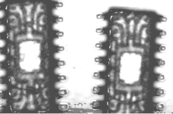
Figure
3
C-SAM image of PEM with die-attach
delaminations (white area)
and poor material porosity causing fuzzy
image.
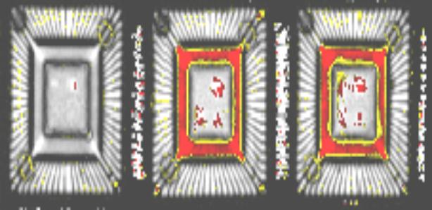
Figure
4
C-SAM images of PEM with delaminations
(Red area)
Figure 5
C-SAM images of PEMs.
Top images show
delaminations (Red area).
Bottom images show porosity in–texture appearance
is mottled.
Figure 6
C-SAM image of
PEM with poor die-attach (Red area)
and delaminations (Yellow/Red area)
Figure 7
C-SAM image of
PEM with poor die-attach.
Appears voided (Red area) and material has
excessive porosity causing fuzzy image.
Figure 8
Construction
analysis photo of PEM.
Wire-bond displacement weakening bond causing latent
dis-bond failure.
Figure 9
C-SAM image of
PEM. “Pop-corning” effect
caused damaged corner from vapor phase solder
re-flow overheating.
Figure 10
Construction
analysis Photo of PEM. “Pop-Corning” effect
caused crack in plastic from
vapor phase solder re-flow overheating.
Figure 11
SEM photo of PEM. Contamination - Residue from
halogen presence in package.
Cause latent defect by accelerating corrosion
and weakening bond.
Figure 12
Photo of PEM
following Salt Spray test. Failures from excessive lead damage.
Caused by
Salt Spray.
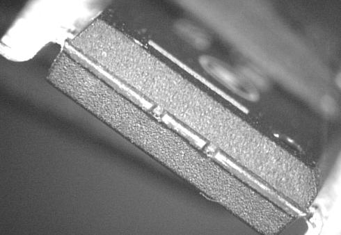
Figure 13
Photo of PEM. Loss of seal integrity
at leadframe tabs of PEM.
Allowed moisture/salt ingression during salt
spray
Test. Accelerated corrosion latent defect.
Figure 14
C-SAM image of
PEMs.
Salt ingression into PEM following Salt Spray test. Cause latent
corrosion defect.
Same PEM as Figure 11.
Figure 15
SEM photo of
PEM with Kirkendall Voiding (Purple Plague)
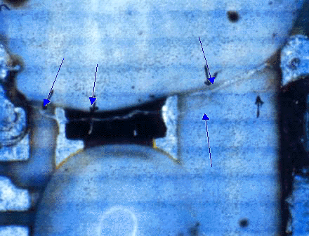
Figure 16
SEM photo of
PEM with internal dendritic growth
Figure 17
C-SAM images
of PEMs with poor die-paddle attachment.
Left images are initial
scans.
Center images are following pre-conditioning.
Right images are
following 50 hours of HAST.
Figure 18
C-SAM images
of PEMs with poor Die-Attach.
Left images are initial scans.
Center
images are following pre-conditioning.
Right images are following 50 hours
of HAST.