c. Using a metal substrate from which the package is
fabricated, is the third method. Two examples are the MQUAD and MBGA packages.
An example of the MQUAD is shown in Figure 2.
In each case, the base of the substrate is made up of an aluminum platebase. The
leads of the MQUAD are stamped leadframes, adhesively attached to the aluminum
plate. After the die-attach, a cover plate is attached. The aluminum base is
exposed to facilitate heatsink attach. The junction to case thermal resistance
can be kept to less than 1.8°C/watt.
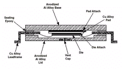
Figure 2. Cavity Down MQUADâ
Package
d. Reducing junction-to-case thermal resistance of a
package that uses a PCB substrate, such as a PPGA or PBGA, is the fourth method.
The chip cavity is punched out and the substrate is laminated to a metal base.
The chip is attached directly to the metal base, with a very low
junction-to-case thermal resistance. High performance PPGA and PBGA packages can
have a junction-to-case thermal resistance of less than 1°C/watt,
primarily limited to the die attach conditions.
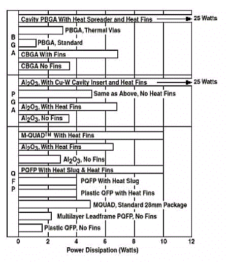
Figure 3. Power Dissipation of Various
Packages in Still Air
Maximum Junction Temperature
Maximum junction temperature. Try to design for a
maximum junction temperature of 90°C and an
ambient temperature of 40°C. The
temperature drop between the junction-to-case and case-to-ambient should be
distributed in a way not to harm the chip or its performance. The maximum
temperature drop from junction to ambient should be 50°C. The
total temperature allowed should be 50°C. Of
this, typically 70% is allocated to the case-to-ambient differential, and 30%
allocated to the junction-to-case differential, or 35°C for the
case-to-ambient and 15°C for the
junction-to-case. With this criterion, the maximum power a package can handle
for a given thermal resistance is shown in Figure 3.
For example, if the package has a thermal resistance of 25°C/watt, it
can handle at most 50°C/25°C/watt or
2 watts.
Thermal Resistance
Thermal resistance. heat must be removed from the
chip’s layers, each of which has some level of thermal resistance. Table 1
shows examples of thermal resistance associated with the junction-to-case path.
For a chip 1cm on a side, an example of the partitioning of the thermal
resistance and the resulting temperature drops for a power of 20 watts is shown
in Table 2.
Decreasing thermal resistance of the junction-to-case path is critical when the
power densities approach the 30W/cm2 range. Two approaches used to
minimize junction-to-case thermal resistance are: (1) decreasing the number and
thickness of the layers between the chip and the heat spreader and (2) using a
more effective heat spreader substrate materials with high thermal conductivity,
such as copper, silicon carbide, and aluminum nitride.
|
Description
|
Material
|
Thickness
(cm)
|
k
(W/cm·K)
|
Thermal
Resistance (°C/W)
|
|
Chip
|
Silicon
|
0.075
|
1.5
|
0.05
|
|
Die Attach
|
Silver-Filled Epoxy
Solder
Epoxy
|
0.0025
0.005
0.0025
|
0.008
0.51
0.002
|
0.313
0.0098
1.25
|
|
Ceramic Package
|
Alumina
Copper Tungsten
Aluminum
|
0.08
0.08
0.08
|
0.2
2.48
2.3
|
0.4
0.032
0.035
|
|
Interconnect
|
FR4 Board
Polyimide
|
0.25
0.005
|
0.002
0.002
|
125.0
2.5
|
|
Heat Spreader
|
Copper
Aluminum
|
0.63
0.63
|
4.0
2.3
|
0.158
0.274
|
Table 1. Selected Junction-to-Case
Thermal Resistances
|
Element
|
Thermal
Resistance (°C/W)
|
Temperature
Drop (°C)
|
|
Silicon Die
Silver-filled Epoxy
Ceramic Base
|
0.05
0.3
0.4
|
1
6
8
|
|
Total
Junction-to-Case
|
0.75
|
15
|
Table 2. Layer Contributions to Thermal
Resistance and Temperature Drop for 20 Watts
Extracting Heat
Thermal resistance from case to ambient depends
on: (1) how efficiently the fluid
(typically air) extracts the heat, (2) the heat carrying capacity of the fluid,
and (3) the surface area in contact with the fluid. A heatsink, using vertical
fins, horizontal discs, pins, or convoluted channels can be used to increase the
surface area through which the heat flows. Ultimately, it is a change in
temperature of an air or liquid stream, or a phase change that carries the heat
out. The efficiency of a heatsink is related to how much it is able to raise the
temperature of the fluid with which it is in contact. The closer the out-flowing
fluid temperature is to the case temperature, the more efficient the heatsink
is. The surface area and the design of the heatsink will clearly play a role in
influencing the efficiency. How much heat can be extracted per unit area from a
surface, in W/cm2, by a heatsink depends on its efficiency, the
surface area of contact, the thermal properties of the fluid, and the volumetric
flow rate. These interact in a very complex manner. Heatsinks are usually
designed with a surface area much larger than the heat generating surface area,
typically by a factor of two to five. The most efficient heat exchanger cannot
extract any more heat than can be carried by the heat capacity of the fluid. The
volumetric flow rate and specific heat of the cooling medium set the
ultimate-power extraction capability for the most efficient heatsinks. If the
heatsink were 100% efficient in heating the air up to the case temperature, the
effective thermal resistance would be at best 50°C/W for
1in 3 /sec of airflow. If the airflow were to double, the thermal resistance
would halve. This assumes perfect efficiency of raising the air up to the case
temperature. In practice, heatsinks are not much more than 50% efficient and the
thermal resistance for air-cooled systems is never less than 100°C/W for
1in3 /sec of airflow.
Substrate Heat
For circuit boards that have only a few high power
components, a significant amount of heat can flow into the substrate, with the
circuit board acting as a giant heat spreader and fin. The better the thermal
transfer through the leads into the board, the more effective the motherboard
will be in cooling. For example, a 119 pin BGA, with the balls under the chip,
can sink over 85% of the total power into the substrate. For this BGA, the
decrease in thermal resistance will be about halved. A thicker board with more
power and ground layers can better function as a heatsink. The substrate is only
going to be effective when there is good thermal contact between the package and
board, when the board has thick power and ground planes and when there are not
many other high power devices nearby. When these conditions are met, the thermal
resistance between the junction and ambient can be reduced by 50%.
Electrical Power Dissipation
Two sources of power dissipation important among all
microcircuit families, is DC or quiescent power dissipation, and AC or switching
power dissipation that increases with switching frequency. The DC power
dissipation is high for ECL but nearly zero for CMOS. The AC power dissipation
can be comparable in both technologies. They are described below:
a. DC Power
and Speed Tradeoffs in ECL electrical power is dissipated only when current
flows through a resistive element. This occurs in steady state, as with pull-up,
pull-down, or terminating resistors, and when current flows through a buffer
transistor during the transient charging and discharging of a capacitor. A
capacitor can be an input gate, on-chip metallization, or output load
capacitance. Modern ECL gates are biased on a steady current value using a
current source. The bias current value is chosen based on a balance between the
DC power dissipation and switching speed. In ECL circuits, the bias current is
what charges or discharges an inter-connect to change its voltage level. To
switch faster, a higher DC current level is required. This higher current also
means more DC power dissipated. In many ECL gate array families, the designer
can select the bias current level to trade off speed and power as appropriate.
b. CMOS
output drivers are never both on simultaneously in the DC mode. When the
microcircuit is set to output high, the p gate is on, and the output is
effectively switched to the VDD rail. When the microcircuit is set
for output low, the output is effectively switched to the VSS rail,
which is typically ground. In typical high speed CMOS circuits, the output load
is capacitive. There may be a series resistor acting as a source termination or
damping resistor, but the DC resistance of the load is typically very high. At
steady state, there is no current flow out of the driver, either through the n
or p transistors. In DC, when the microcircuit is not switching, there is very
little power dissipation in a CMOS microcircuit.
Because of the nature of RC circuits, all the stored
energy will be converted Into heat energy each time the capacitance is either
charged or discharged. This power
dissipation depends on the switching voltage, the gate capacitance, and the
switching or clock frequency. Because of the voltage squared dependence,
decreasing the switching voltage can have a large impact on decreasing the power
consumption. For example, at 1-micron channel length, the typical power
consumption of a 5V CMOS gate is approximately 6µW/MHz/gate for internal gates.
If the voltage were dropped to 3V, the power consumption would drop to
2.2µW/MHz/gate. In addition, the area of
the gate contributes to the gate capacitance. Reducing the feature size also
reduces the gate capacitance. However, the gate oxide thickness is also reduced,
which acts to increase the gate capacitance. The net result of decreased feature
size is still a reduction of power dissipation. For 0.5 micron CMOS, operating
on 3V supplies, the gate power dissipation is roughly 1.5µW/MHz/gate. At 100MHz, the power dissipation per
internal gate for 1 micron CMOS would be 0.6mW/gate. Because of the larger size
of output drivers, power consumption would be roughly 2.4mW/gate. This is
comparable to ECL DC power dissipation. However in CMOS, it is only those gates
actually switching that contribute to the power dissipation. For example, a
50,000-gate array, with 20 percent of the internal gates switching per cycle and
50 output drivers switching per cycle, would dissipate:
PAC = (6µW x 10,000) + (24µW x 50) =
61.2mW/MHz.
If each of the output gates drives a 25pF load, the
dissipation would be an additional 30mW/MHz. The total power dissipation at
100MHz, for example, would be nine watts for a CMOS microcircuit. An advantage of CMOS technology is the
absence of DC power dissipation.
However, AC power-dissipation increases with frequency.
Minimizing Power Consumption
Four ways to minimize power consumption are: (1)
Design for low power consumption. (2) Reduce the supply voltage. Lowering the
supply voltage has the benefit of reducing power but also slows the switching
speed. (3) Use smart power management. Smart power management uses specialized
chips that monitor the CPU activity level. As the activity level drops, the
clock frequency is slowed down. In effect, smart power management puts the
system to sleep between keystrokes or other activities. (4) Adjust the clock
frequency to slowdown when the application is not in use.
GaAs Integration
To keep power dissipation under control, the
microcircuit speed has to be limited at high integration levels or the
microcircuit gets too hot. There is a
trade-off between speed and integration with GaAs microcircuits. If the
integration levels are high, speed must be contained; if the speed is high,
integration levels must be contained.