Download the PDF file
Wirebonding
Gold and aluminum are two types of wire typically
used for wirebonding. Each has a different assembly process, equipment and
operating conditions. The metallization on the chip is typically aluminum and
the metallization on the second pad is typically gold or silver plated copper.
The bonding is performed at room temperature and the weld is accomplished with
pressure and ultrasonic energy. When just heat and pressure is used the process
is termed thermocompression bonding. In order to form a reliable gold-aluminum
bond, the joint temperature must be in the 300-400°C range.
This is suitable for ceramic packages using a Si-Au eutectic die attach but is
too hot for plastic packages. When lower temperatures are required, the addition
of ultrasonic energy reduces the temperature required for reliable joint
formation to 150-200°C. This
process is termed thermosonic bonding. In addition to the temperature difference
between gold and aluminum wirebonding, the other chief difference is the speed
of the bonding.
Gold Thermocompression Bonding
Gold thermocompression bonding is 3 - 5 times faster
than aluminum wedge bonding. The speed advantage is due to the nature of the
motion of the tool and the substrate. When the ball-bond is formed on the die,
the tool can move off in any direction to make the second bond. The package or
substrate can be stationary and the tool goes back and forth. This means the
bonding process is limited by how fast the tool can move from pad to pad.
High-speed bonders can process 10 bonds per second.
Aluminum Wedge Bonding
For Aluminum wedge bonding the tool is directional.
The first and second wedge bond must be done in the direction of the wire. In
most packages, the wirebonds fan out. After each bond is made the tool head must
be rotated slightly. This slows down the bonding process to only about 3 bonds
per second. When the bonds are parallel, and the tool does not have to rotate,
ultrasonic aluminum wedge bonding will be faster than 3 bonds per second.
Chip bond
Important electrical properties of the chip bond are
lead inductance and resistance. The most important influence on the lead
inductance is length. The shorter the interconnect, the lower the inductance.
Lower inductance in the power and ground path will decrease ground bounce and
switching noise. The second important term is resistance. Resistance will affect
the DC voltage drop in power and ground paths. A wirebond, 1mil in diameter has
a resistance of about 1 Ohm/inch. For a wire 50 mils long, the resistance is
about 50 mOhms. With the typically 0.25 A limit for a single wirebond, the DC
voltage drop might be 12 mV, below the typical noise budget for even a 3 V
system. Shorter lengths and wider cross sections contribute to lower resistance.
Typical electrical properties of various interconnect are summarized in Table 3.
Table
3. Summary of Electrical
Properties of Chip Bonding
|
|
Resistance Per Length
|
Inductance Per
Length
|
Typical Lengths
|
Typical Resistances
|
Typical Inductances
|
|
Wirebond
|
1 Ohm/inch
|
25nH/inch
|
50-100mils
|
50-100mOhms
|
1.2-2.5nH
|
| TAB
|
|
21nH/inch
|
100-300mils
|
25-75mOhms
|
2.1-6.3nH
|
| Flip Chip
|
0.08 Ohms/inch
|
18nH/inch
|
3-6mils
|
<
1mOhm
|
<
0.1nH
|
Pad Counts
Pad counts for die continue to increase. This comes
from the combination of increased functionality and gate count, and the need for
more power and ground pins to minimize ground bounce. The die-size for the same
gate count is decreasing as the feature size gets smaller. These factors
contribute to the need to decrease the pad pitch required around the periphery
of a die for bonding pads. For example, the Pentium chip has maintained the same
functionality, yet has gone through a number of die shrinks as the feature size
has been reduced. The die shrink is illustrated
in Figure 3.
Though the die got smaller, the number of I/O off the die stayed the same. This
means the bond pad pitch has to shrink.
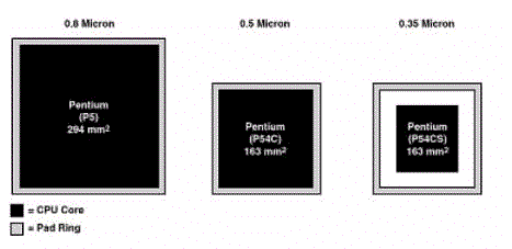
Figure 3. Intel Shrinks
Pentium
Pad Pitch
The microcircuit manufacturing process can make pads
on 1-micron centers. The useful pitch of a bonding pad is set by the wirebonder
technology. This is the major driving force on bonding technology allowing a
tighter pad pitch on the chip. Figure 4
shows the maximum number of pads that can fit on a die with a fixed pad pitch.
For the largest die, at 18mm on a side, the pad limited I/O count is 720 I/O for
100 micron centers. A growing concern for large ASICs is being pad limited. This
means the die size must be artificially increased to allow enough perimeter for
all the bonding pads.
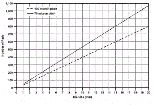
Figure 4. Maximum
I/O Possible for Pads Limited Peripheral Die
Source:
ICE, “Roadmaps of Packaging Technology”
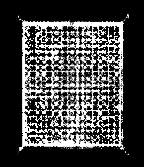
Die Pad/Paddle Design
| WAFFLE PATTERNED DIE PAD |
PLAIN SURFACE DIE PAD |
| ( PREFERRED DESIGN ) |
( PRONE TO DISATTACH ) |
|
|
 |
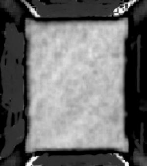 |
Acoustic Microscopy
Images
The surface texture of Pad/paddle designs that
accommodate large die, now common in quad-flatpacks, needs to provide an
adhesive enhancing feature to insure adequate strength to withstand the stresses
of the solder re-flow process. The stress of solder re-flow temperature from the
difference in TCE between the die, the die paddle and the encapsulant, is
compounded by the moisture absorption properties of the plastic. The vapor
pressures generated at the smooth surface interface are distributed entirely
against the die forcing it away from the paddle. This results in a weakening or
de-laminating of the die attach interface and poor thermal conductivity is a
result. Poor thermal conductivity often results in excessive heating of the die
causing electrical parameter failures. Mechanical movement of the die also can
result in broken bond wires.
The waffle design in the acoustic microscopy image
above is a popular, but more costly, alternative to the plain surface design.
The waffle design provides more surface area for better adhesion and allows for
some expansion of the vapors during solder
re-flow.